Semiconductor assembly and manufacturing method thereof

A manufacturing method and semiconductor technology, applied in semiconductor/solid-state device manufacturing, semiconductor devices, semiconductor/solid-state device components, etc., can solve problems such as manufacturing yield reduction and circuit short circuit

Active Publication Date: 2015-04-15
ADVANCED SEMICON ENG INC
View PDF5 Cites 1 Cited by
  • Summary
  • Abstract
  • Description
  • Claims
  • Application Information

AI Technical Summary

Problems solved by technology

[0004] However, due to the plasma etching of the passivation layer, a ring groove will be formed on the periphery of the through-silicon via (TSV), and when the etching is over-etched, the ring groove will easily extend to the wafer surface, causing the energy of the plasma to flow along the TSV. The ring groove contacts the surface of the wafer to produce a partial discharge effect, which causes the circuit of the wafer (such as the circuit on the other side of the active surface) to be short-circuited, resulting in a decrease in manufacturing yield

Method used


Image

  • Semiconductor assembly and manufacturing method thereof
  • Semiconductor assembly and manufacturing method thereof
  • Semiconductor assembly and manufacturing method thereof

Examples


Embodiment Construction

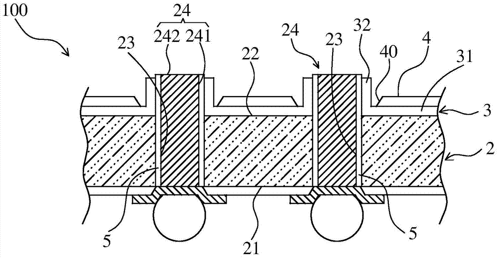
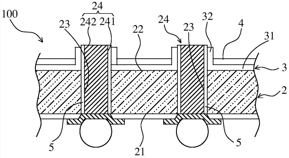
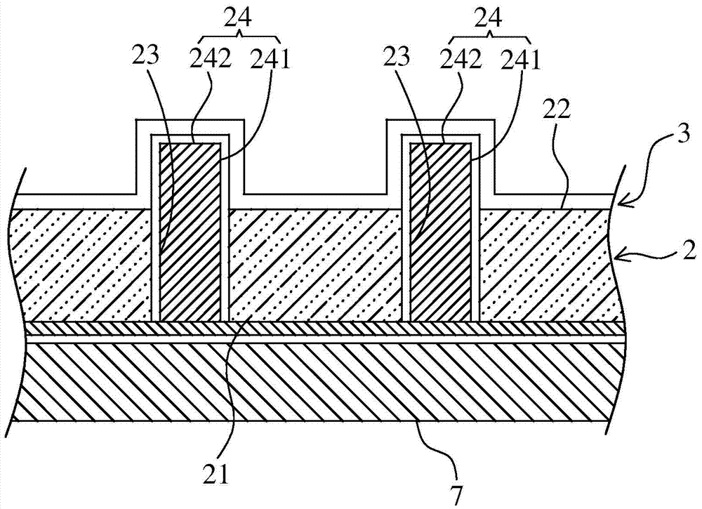
[0016] The following descriptions of the various embodiments refer to the accompanying drawings to illustrate specific embodiments in which the present invention can be practiced. Furthermore, the directional terms mentioned in the present invention are, for example, up, down, top, bottom, front, back, left, right, inside, outside, side, surrounding, central, horizontal, transverse, vertical, longitudinal, axial, The radial direction, the uppermost layer or the lowermost layer, etc. are only directions referring to the attached drawings. Therefore, the directional terms used are used to illustrate and understand the present invention, but not to limit the present invention.

[0017] Please refer to figure 1 As shown, the semiconductor device 100 according to an embodiment of the present invention mainly includes a silicon substrate 2 , a first passivation layer 3 and a second passivation layer 4 . The present invention will describe in detail the detailed structure, assembly...


PUM


Abstract

The invention discloses a semiconductor assembly and a manufacturing method thereof. The semiconductor assembly comprises a silicon substrate, a first passivation layer, and a second passivation layer. The silicon substrate comprises a plurality of silicon through-vias and a plurality of conductive columns. The first passivation layer comprises a flat portion and an annular portion. The height of the annular portion is lower than the height of the top surface of the conductive column. The second passivation layer is covered on the first passivation layer. The height of the second passivation layer is lower than the height of the annular portion of the first passivation layer. Through arranging the first passivation layer and the second passivation layer on the back surface of the silicon substrate, after etching, the first passivation layer still wraps the back surface of the silicon substrate, reducing possibility that the first passivation layer is etched too deep and extends to the back surface of the silicon substrate, so as to reduce circuit short circuit risk of a semiconductor assembly finished product and improve manufacturing yield rate.

Description

technical field [0001] The present invention relates to a semiconductor component and its manufacturing method, in particular to a semiconductor component provided with two passivation layers with different etching rates and its manufacturing method. Background technique [0002] Nowadays, the electronic product design industry is moving towards the trend of lightness, thinness, and shortness, and semiconductor packaging technology has also developed packaging technologies such as stacked semiconductor element packaging. The semiconductor elements are packaged in the same packaging structure, so that the packaging density can be increased to reduce the size of the package body, and the three-dimensional stacking can be used to shorten the signal transmission path between the semiconductor elements, so as to increase the signal transmission speed of the semiconductor. At present, the existing stacked semiconductor device packaging manufacturing method is to stack chips on a w...

Claims


Application Information

Patent Timeline
Patent Type & Authority Applications(China)
IPC IPC(8): H01L23/485H01L21/60
CPCH01L2224/11
Inventor 蒋源峰黄敏龙
Owner ADVANCED SEMICON ENG INC
Why Eureka
Try Eureka