Metal micro-/nano-sensing device

A technology for sensor devices and metals, which is applied in the field of metal micro-nano sensor devices, can solve the problems of low detection efficiency and low detection sensitivity, and achieve the effects of improving detection efficiency, expanding sensitive areas, and enhancing electromagnetic field distribution

Inactive Publication Date: 2015-04-22
NINGBO UNIVERSITY OF TECHNOLOGY
View PDF2 Cites 3 Cited by
  • Summary
  • Abstract
  • Description
  • Claims
  • Application Information

AI Technical Summary

Problems solved by technology

However, in this type of structure, the strong electromagnetic field is only distributed in the gaps of the nanoparticles, and the size is generally around 10nm, so it is only suitable for the detection of trace samples, the detection sensitivity is not high, and the detection efficiency is low

Method used


Image

  • Metal micro-/nano-sensing device
  • Metal micro-/nano-sensing device
  • Metal micro-/nano-sensing device

Examples


Embodiment 1

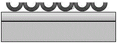
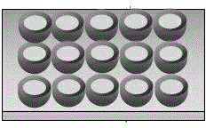
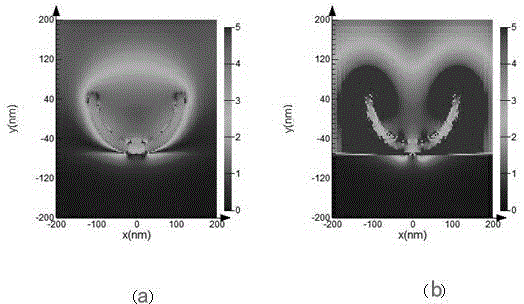
[0024] Embodiment 1: see figure 1 to Figure 5 Shown is a specific embodiment of the metal micro-nano sensor device of the present invention. The thickness of the metal Au film in the sensor is 100nm, the radius of the metal Au hemispherical shell is 100nm, the thickness of the shell is 20nm, and the metal hemispherical shells are arranged in a square with a period of 240nm. Compared image 3 with Figure 4 , only the electromagnetic field distribution of the metal nano-shell when it is excited under resonance conditions. It can be seen that the introduction of the metal film greatly improves the electromagnetic field distribution around the metal hemispherical shell, not only between the metal film and the metal nano-shell, but also in the metallic spherical shell. A strong resonant electromagnetic field distribution is also formed in the cavity. pass Figure 5 The reflection spectrum of the theoretically simulated sensor in different refractive index environments can b...

Embodiment 2

[0025] Example 2: see figure 1 to Figure 4 ,as well as Image 6 Shown is a specific embodiment of the metal micro-nano sensor device of the present invention. The thickness of the metal Au film in the sensor is 100nm, the radius of the metal Au hemispherical shell is 100nm, the thickness of the metal Au hemispherical shell is 20nm, and the hemispherical shells are arranged in a square with a period of 480nm. Compared image 3 with Figure 4 , only the electromagnetic field distribution of the metal nano-shell when it is excited under resonance conditions. It can be seen that the introduction of the metal film greatly improves the electromagnetic field distribution around the metal hemispherical shell, not only between the metal film and the metal nano-shell, but also in the metallic spherical shell. A strong resonant electromagnetic field distribution is also formed in the cavity. pass Image 6 The reflection spectrum of the theoretically simulated sensor in different ...

Embodiment 3

[0026] Embodiment 3: see figure 1 to Figure 4 ,as well as Figure 7 Shown is a specific embodiment of the metal micro-nano sensor device of the present invention. The thickness of the metal Au film in the sensor is 100nm, the radius of the metal Au hemispherical shell is 50nm, and the thickness of the metal Au hemispherical shell layer is 20nm. The metal hemispherical shells are arranged in four directions with a period of 140nm. Compared image 3 with Figure 4 , only the electromagnetic field distribution of the metal nano-shell when it is excited under resonance conditions. It can be seen that the introduction of the metal film greatly improves the electromagnetic field distribution around the metal hemispherical shell, not only between the metal film and the metal nano-shell, but also in the metallic spherical shell. A strong resonant electromagnetic field distribution is also formed in the cavity. pass Figure 7 The reflection spectrum of the theoretically simula...


PUM

PropertyMeasurementUnit
thicknessaaaaaaaaaa
radiusaaaaaaaaaa
thicknessaaaaaaaaaa

Abstract

The invention discloses a metal micro-/nano-sensing device and belongs to the field of photoelectric sensors. The device comprises a silica substrate layer, wherein a metal film is arranged on the silica substrate; a metal hemispherical shell is arranged on the metal film; and the metal hemispherical shell is periodically arranged on the metal film. Compared with the prior art, the metal micro-/nano-sensing device disclosed by the invention has the advantages that large-area and high-intensity electromagnetic field distribution is obtained by virtue of the coupling action of the metal film and the metal micro-/nano hemispherical shell, and the metal micro-/nano-sensing device is sensitive to the near-field refractive index change, can operate in a near-infrared band, easily realizes monolithic integration and has good application prospects in the fields of biology, medicines and chemical sensors.

Description

technical field [0001] The invention belongs to the field of photoelectric sensors, in particular to a metal micro-nano sensor device. Background technique [0002] Metal surface plasmons (SPR) are electromagnetic oscillations that propagate along the metal-dielectric interface. The SPR resonance of metal thin films is sensitive to the near-field refractive index, and has outstanding advantages such as high sensitivity, label-free, real-time, and rapid detection. In the early 1990s, the Swedish Biacore AB company successfully developed a commercial SPR analyzer. Since then, SPR biochemical sensing technology has developed rapidly and has been widely used in the fields of biology, chemistry, environment, medical treatment, food and pharmaceuticals. However, traditional SPR sensors based on metal thin films often require optical elements such as prisms to excite surface plasmon waves. Therefore, the structure of the sensor is complex and bulky, making it difficult to achieve ...

Claims


Application Information

Patent Timeline
Patent Type & Authority Applications(China)
IPC IPC(8): G01N21/41G01N21/65
Inventor 程培红
Owner NINGBO UNIVERSITY OF TECHNOLOGY
Why Eureka
Try Eureka