
High-speed ingaas photodetector chip flip-chip integration structure and manufacturing method

A technology of photodetector and manufacturing method, which is applied in the direction of circuits, electrical components, semiconductor devices, etc., to achieve the effect of increasing the light receiving aperture, simple and applicable structural design, and reducing the influence of parasitic inductance

Active Publication Date: 2017-03-08
THE 44TH INST OF CHINA ELECTRONICS TECH GROUP CORP
View PDF3 Cites 0 Cited by
  • Summary
  • Abstract
  • Description
  • Claims
  • Application Information

AI Technical Summary

Problems solved by technology

However, the back-illuminated 10Gb / s PIN-PD or APD die needs to be flip-chip integrated to meet subsequent packaging requirements

Method used


Image

  • High-speed ingaas photodetector chip flip-chip integration structure and manufacturing method
  • High-speed ingaas photodetector chip flip-chip integration structure and manufacturing method
  • High-speed ingaas photodetector chip flip-chip integration structure and manufacturing method

Examples


Embodiment approach

[0048] As an implementation, the manufacturing process of the first metal pad, the second metal pad, the P electrode bonding pad and the N electrode bonding pad, that is, the P and N metal electrode patterns on the carrier includes: firstly adopt The magnetron sputtering method grows the TiW / Au metal film layer in sequence, with a thickness of 100nm / 500nm; and then adopts the photolithography lift-off process to define the evaporation area of ​​the P and N metal electrodes on the sapphire substrate. Methods Thicken the Au layer to 3 microns; then remove the TiW / Au metal film layer outside the P and N metal electrode patterns by wet etching; finally complete the sapphire substrate with P and N metal electrode patterns. Specifically, on the sapphire substrate (thickness 250 microns), the TiW / Au metal film layer is sequentially grown by magnetron sputtering to form an initial seed (seed) layer, and the thickness requirement is 100 nanometers / 500 nanometers; Then use high-resoluti...


PUM


Abstract

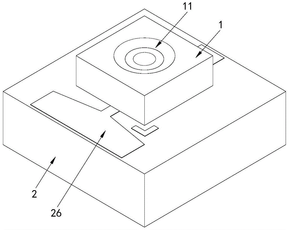
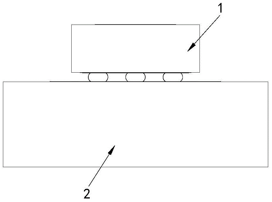
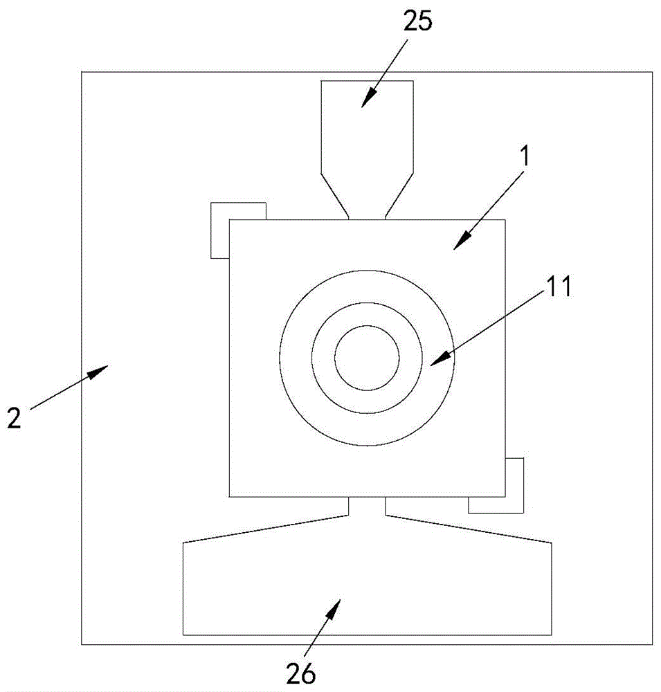
The invention provides an integrated structure for inversely installing a high-speed InGaAs photoelectric detector chip. The integrated structure comprises a tube core and a carrier used for welding the tube core in an inversely-installed mode. A micro-lens is integrated on the substrate face of the tube core. A P electrode is arranged in the center of the front of the tube core. N electrodes are symmetrically arranged in the center of the front. A first metal welding pad corresponding to the P electrode is arranged in the center of the front of the carrier. Second metal welding pads corresponding to the N electrodes are symmetrically arranged in the center of the front. The first metal welding pad is provided with a first metal protruding point bonding with the P electrode. The second metal welding pads are provided with second metal protruding points bonding with the N electrodes. The front of the carrier is provided with a P electrode bonding welding pad bonding with a gold wire of the first metal welding pad, and N electrode bonding welding pads bonding with gold wires of the second metal welding pads. The invention further provides a manufacturing method. The integrated structure is simple and applicable in structure, and can achieve the effects of the photoelectric property and the structural reliability of the tube core with the chip installed inversely.

Description

technical field [0001] The invention belongs to the technical field of semiconductors, and in particular relates to a high-speed InGaAs photodetector chip flip-chip integration structure and a manufacturing method. Background technique [0002] With the continuous development of optical fiber communication technology, 10Gb / s and above high-speed optical fiber communication network has been developed rapidly and widely used. 10Gb / s InGaAs / InP PIN photodiode (PIN-PD) or avalanche photodiode (APD) is used for receiving and detecting high-speed optical signals, and is one of the core chips in 10Gb / s and above high-speed optical fiber communication. [0003] The existing 10Gb / s rate and above PIN-PD or APD die adopts the vertical incident light on the front, and the P and N electrodes have different surface structures. The ohmic contact on the front of the chip and the contact ring of the P electrode occupy the active area, resulting in a small light receiving aperture of the chi...

Claims


Application Information

Patent Timeline
Patent Type & Authority Patents(China)
IPC IPC(8): H01L31/09H01L31/18
CPCH01L31/0224H01L31/02327H01L31/09H01L31/1844Y02P70/50
Inventor 崔大健高新江黄晓峰樊鹏董绪丰
Owner THE 44TH INST OF CHINA ELECTRONICS TECH GROUP CORP
Learn More