Broadband THz wave plate composed of specific electromagnetic surface
A special surface and wave plate technology, applied to electrical components, antennas, polarizing components, etc., can solve problems such as difficult to achieve refractive index
- Summary
- Abstract
- Description
- Claims
- Application Information
AI Technical Summary
Problems solved by technology
Method used
Image
Examples
Embodiment Construction
[0024] For the ultra-broadband THz wave plate, it is divided into two parts: the preparation process and the measurement process.
[0025] 1. Preparation of ultra-broadband THz wave plate:
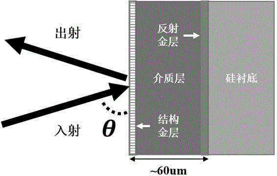
[0026] According to the parameters about the whole system optimized by numerical simulation, the designed samples are prepared by using micro-nano processing technology. The main preparation steps include:
[0027] (1) Clean the silicon wafer, and evaporate 50nm gold on it by electron beam evaporation.
[0028] (2) Slice the silicon wafer with the evaporated gold layer into a size of 1.2cm*1.2cm, paste a layer of adhesive tape (polyimide resin film) on it, the thickness is about 60um, and the power saving parameter of the dielectric layer is about ε =3.1+0.04i.
[0029] (3) Apply LOR (polybutylene oxime) at 4000rpm, dry at 180° for about 3 minutes, apply photoresist AZ5214 at 5000 rpm, and dry at 95° for 90s.
[0030] (4) Use UPG501 plate making machine to directly write the designed s...
PUM
| Property | Measurement | Unit |
|---|---|---|
| Thickness | aaaaa | aaaaa |
| Width | aaaaa | aaaaa |
Abstract
Description
Claims
Application Information


