Eureka AIR delivers breakthrough ideas for toughest innovation challenges, trusted by R&D personnel around the world.

Method and device for removing metal impurities in polycrystalline silicon by electron beam overheat smelting

A metal impurity, polysilicon technology, applied in the metallurgical field, can solve the problems of wasting electricity and long production time, and achieve the effect of reducing the purification process, the number of times, and the production cost.

Inactive Publication Date: 2015-04-29
DALIAN UNIV OF TECH
View PDF2 Cites 6 Cited by
  • Summary
  • Abstract
  • Description
  • Claims
  • Application Information

AI Technical Summary

Problems solved by technology

The directional solidification technology proposes that the processing time is about 1 to 2 days, the production time is longer, and a lot of electricity is wasted in the process of multiple purifications.

Method used


Image

  • Method and device for removing metal impurities in polycrystalline silicon by electron beam overheat smelting

Examples


Embodiment 1

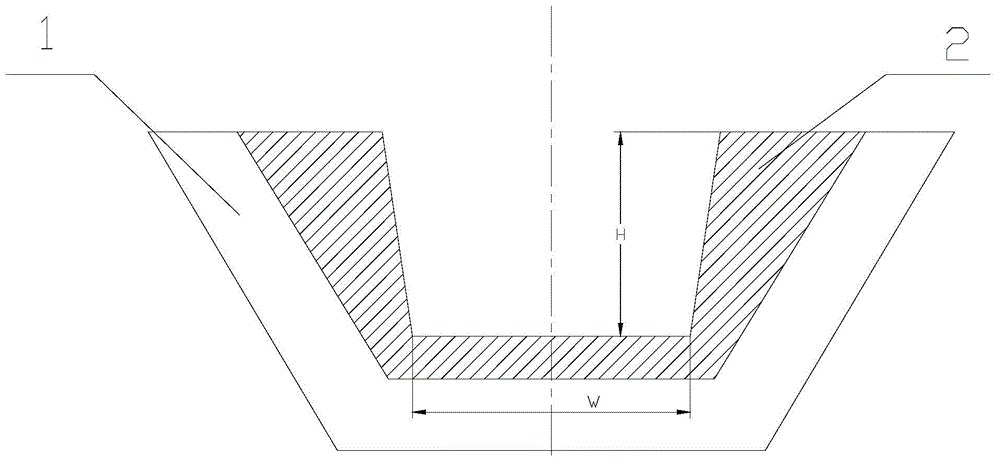
[0025] like figure 1 As shown, an electron beam melting polysilicon device includes a water-cooled melting crucible, the angle between the inner wall of the water-cooled copper crucible and the bottom of the water-cooled copper crucible is 105°, the water-cooled copper crucible is provided with a graphite bushing, and the graphite The outer surface of the liner is attached to the inner surface of the water-cooled copper crucible, the bottom of the graphite liner is horizontal to the bottom of the water-cooled copper crucible, and the angle between the side wall of the inner surface of the graphite liner and the bottom of the graphite liner is 95°.

[0026] The bottom thickness of the graphite bushing is 20mm.

[0027] The thickness of the thinnest part of the side wall of the graphite substrate is equal to 20mm.

[0028] The ratio between the inner height H of the graphite liner and the width W of the bottom is 1:1.

[0029] A method for removing metal impurities in polysili...

Embodiment 2

[0037] like figure 1 As shown, an electron beam melting polysilicon device includes a water-cooled melting crucible, the angle between the inner wall of the water-cooled copper crucible and the bottom of the water-cooled copper crucible is 110°, the water-cooled copper crucible is provided with a graphite bushing, and the graphite The outer surface of the liner is attached to the inner surface of the water-cooled copper crucible, the bottom of the graphite liner is horizontal to the bottom of the water-cooled copper crucible, and the angle between the side wall of the inner surface of the graphite liner and the bottom of the graphite liner is 97°.

[0038] The bottom thickness of the graphite bushing is 30mm.

[0039] The thickness of the thinnest part of the side wall of the graphite substrate is equal to 20mm.

[0040] The ratio between the inner height H of the graphite liner and the width W of the bottom is 1.5:1.

[0041] A method for removing metal impurities in polysi...

Embodiment 3

[0049] like figure 1 As shown, an electron beam melting polysilicon device includes a water-cooled melting crucible, the angle between the inner wall of the water-cooled copper crucible and the bottom of the water-cooled copper crucible is 120°, the water-cooled copper crucible is provided with a graphite bushing, and the graphite The outer surface of the liner is attached to the inner surface of the water-cooled copper crucible, the bottom of the graphite liner is horizontal to the bottom of the water-cooled copper crucible, and the included angle between the side wall of the inner surface of the graphite liner and the bottom of the graphite liner is 100°.

[0050] The bottom thickness of the graphite bushing is 40mm.

[0051] The thickness of the thinnest part of the side wall of the graphite substrate is equal to 20mm.

[0052] The ratio between the inner height H of the graphite liner and the width W of the bottom is 2:1.

[0053] A method for removing metal impurities i...


PUM


Abstract

The invention discloses a method and device for removing metal impurities in polycrystalline silicon by electron beam overheat smelting, and belongs to the field of metallurgy. The device comprises a water-cooled copper smelting crucible, wherein an inclined sidewall design is adopted for the water-cooled copper smelting crucible; the inner sidewall of the water-cooled copper smelting crucible forms an included angle of 105 to 120 degrees with the bottom of the water-cooled copper smelting crucible; a graphite bushing is arranged in the water-cooled copper smelting crucible; the outer surface of the graphite bushing is attached to the inner surface of the water-cooled copper smelting crucible to form a close fit design; the bottom of the graphite bushing and the bottom of the water-cooled copper smelting crucible are horizontal, the inner surface sidewall of the graphite bushing forms an included angle of 95 to 100 degrees with the bottom of the graphite bushing. According to the device, the metal impurities are removed by overheat smelting, so that the number of times of subsequent directional solidification and ingot casting can be reduced, a purification process can be eliminated, and the production cost can be reduced; by electron beam overheat smelting for polycrystalline silicon purification, post directional solidification can be reduced by one time or more, and the metal impurities in the polycrystalline silicon can be reduced by 30 percent or more.

Description

technical field [0001] The invention relates to a method for removing metal impurities in polysilicon by electron beam overheating melting, which belongs to the field of metallurgy. Background technique [0002] The preparation of solar-grade polysilicon by metallurgical method is currently widely promoted and adopted due to its low cost, low energy consumption, and environmental friendliness. In the purification process, according to the existence form of impurities in polysilicon and the physical and chemical properties of each impurity element, boron impurities in polysilicon are mainly removed by slagging and smelting, and by directional solidification (ingot) or pickling. Metal impurities in polysilicon, phosphorus impurities in polysilicon are removed by electron beam melting or vacuum melting. [0003] Currently, for polysilicon with a total concentration of metal impurities exceeding 1000 ppmw, two or more directional solidification techniques are required to reduce...

Claims


Application Information

Patent Timeline
IPC IPC(8): C01B33/037
Inventor 姜大川石爽王登科谭毅
Owner DALIAN UNIV OF TECH
Why Eureka
Eureka Blog
Learn More