
ESD (Electro-Static discharge) electrostatic protection structure for IO Pad

A static protection, MOS tube technology, applied in the direction of circuits, electrical components, electrical solid devices, etc., can solve the problems of improving the anti-static ability of ESD devices, large occupation area, and large layout area of ​​IOPad, so as to facilitate the popularization of design And improvement, obvious area advantages, and the effect of reducing the process flow

Active Publication Date: 2015-04-29
BEIJING MXTRONICS CORP +1
View PDF9 Cites 6 Cited by
  • Summary
  • Abstract
  • Description
  • Claims
  • Application Information

AI Technical Summary

Problems solved by technology

Existing chips generally adopt the IO Pad electrostatic protection structure provided by the process manufacturer. The ESD protection devices are composed of specially designed ESD Device devices. The specific process flow, fixed layout structure and fixed size occupy a large area on the layout. , is one of the main reasons for the large layout area of ​​the IO Pad, resulting in high cost; at the same time, non-standard MOS device design is not easy to carry out compatible design of other processes, and it is not easy to improve the anti-static ability of ESD devices

Method used


Image

  • ESD (Electro-Static discharge) electrostatic protection structure for IO Pad
  • ESD (Electro-Static discharge) electrostatic protection structure for IO Pad
  • ESD (Electro-Static discharge) electrostatic protection structure for IO Pad

Examples


Embodiment Construction

[0019] The ESD electrostatic protection structure of the IO Pad according to the present invention will be described in further detail below in conjunction with the accompanying drawings and specific embodiments.

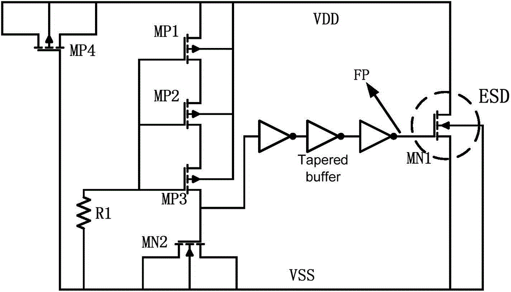
[0020] Such as figure 1 Shown is the ESD protection circuit diagram of the existing power supply PAD. The ESD protection device in this circuit is an N-type MOS transistor MN1, which serves as a discharge path for charges, and its source and drain terminals are respectively connected to the ground and the power supply. The ESD detection circuit is composed of P-type MOS transistors MP1~MP4, MN2 and resistor R1, wherein the inverse proportional MOS transistors MP1~MP3 are used as resistors in series, and the source and drain regions of P-type MOS transistors MP4 and MN2 are connected as capacitors. When the power supply voltage works normally and is stable, the P-type MOS transistor MP4 does not form a path, the gate terminals of the P-type MOS transistors MP1~MP3 h...


PUM


Abstract

The invention provides an ESD (Electro-Static discharge) electrostatic protection structure for an IO Pad. The structure comprises a substrate, two P type transistors, four N type transistors, an isolating resistor, two PAD channels and an N type well region. The structure adopts a non-ESD device to form a protection device, and adopts finger-shaped MOS tube units connected in parallel to form MOS tube parallel groups; a plurality of the MOS tube parallel groups are distributed side by side to form a large-sized electrostatic protection MOS device; a double-PAD channel adopted for layout planning and the double-PAD channel, an ESD protection N type MOS device region, and a P type MOS device are distributed at intervals. Compared with an ESD electrostatic protection structure for the IO Pad, provided by a technology producer, the ESD electrostatic protection structure for the IO Pad, provided by the invention, has the benefits that the process is simplified, other process designs are adopted in a compatible manner, so that equivalent electrostatic protection performance is achieved, and at the same time the electrostatic protection device is smaller in size, lower in cost, and is more convenient for people to improve the electrostatic protection device for antistatic ability improvement.

Description

technical field [0001] The invention belongs to the technical field of ESD electrostatic protection in integrated circuits, and in particular relates to an ESD electrostatic protection circuit structure of an IO Pad (input and output pin). Background technique [0002] Electrostatic Discharge (ESD) is the main factor that causes most electronic components or electronic systems to be damaged by excessive electrical stress. This damage can cause a permanent damage to the semiconductor components, affecting the circuit function of the integrated circuit. About 30% to 40% of the electrical failures of integrated circuit products are related to ESD electrostatic shocks. With the continuous development of CMOS technology, the feature size of integrated circuits is gradually reduced. When it comes to submicron and deep submicron technology, the gate length, gate oxide layer thickness, junction depth, and epitaxial layer thickness of the device are all reduced accordingly, making ...

Claims


Application Information

Patent Timeline
IPC IPC(8): H01L27/02
Inventor 宗宇査启超赵元富姚全斌冯奕翔宋晶峰
Owner BEIJING MXTRONICS CORP
Learn More