Novel electrode structure of silicon solar cell

A solar cell and electrode structure technology, applied in the field of solar cells, can solve problems such as power reduction, broken grids, and burned out components, and achieve the effect of reducing battery costs

Inactive Publication Date: 2015-04-29
JIANGSU SHUNFENG PHOTOVOLTAIC TECH CO LTD
View PDF5 Cites 3 Cited by
  • Summary
  • Abstract
  • Description
  • Claims
  • Application Information

AI Technical Summary

Problems solved by technology

[0006] Therefore, it is an obvious trend to reduce the width of auxiliary grid lines, but the problem of grid breakage will inevitably occur when the grid line width is reduced, and the thinner the grid line is, the more likely it is to cause grid breakage
This will reduce the probability of collecting minority carriers, resulting in a decrease in the collected photocurrent. After the module is made, it will affect the electrical performance of the entire module, and the power will be reduced. In the future grid-connected power station, due to the hot spot effect in the module, Local heating is too high, which affects the life of the components and seriously burns out the components
like figure 1 In the printed pattern shown, the sixth thin grid line from right to left is broken at two places, causing three grid lines to lose the function of collecting the photocurrent at the position and transporting it to the main grid line. The photocurrent collected by the unit light-receiving area of ​​the photocell thus reducing the performance of the battery

Method used


Image

  • Novel electrode structure of silicon solar cell
  • Novel electrode structure of silicon solar cell
  • Novel electrode structure of silicon solar cell

Examples


Embodiment 1

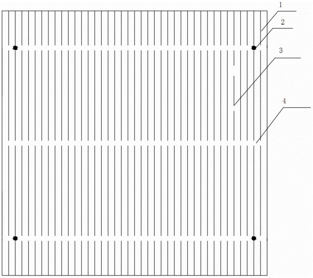
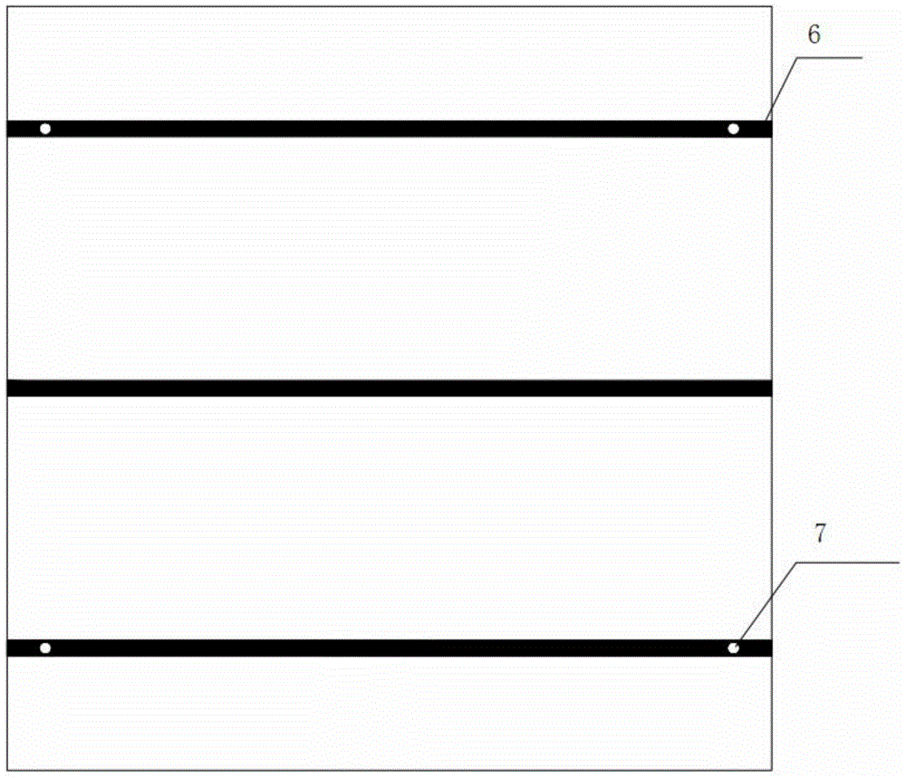
[0021] Such as figure 1 As shown, the front electrode of the crystalline silicon solar cell of the present invention includes three gaps 4 for busbar printing, two parallel sub-grids 5 and more than three vertical sub-grids 1; the gaps 4 for busbar printing are equidistant and Arranged in parallel, the parallel sub-grid lines 5 are parallel to the gap 4 for printing the main grid lines and located in the middle of the two gaps 4, the parallel sub-grid lines 5 connect two adjacent vertical sub-grid lines 1; The width of the grid printing gap 4 is 1.2 mm, the width of the main grid 6 is 1.5 mm, the width of the parallel auxiliary grid lines 5 is 0.05 mm, and the width of the vertical auxiliary grid lines 1 is 0.05 mm.

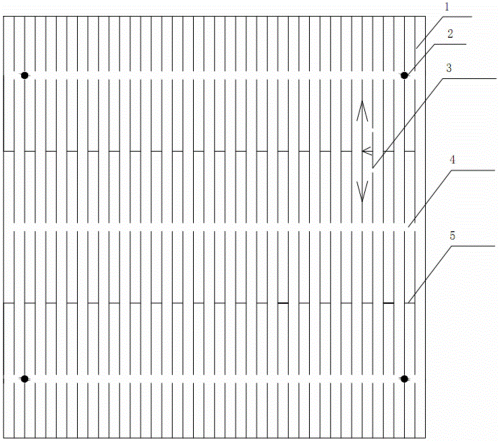
[0022] After this design, the photocurrent collected by the vertical sub-grid at 3 can be as follows image 3 As shown by the middle arrow, it can flow to the gap 4 for the printing of the main grid line through the adjacent vertical fine grid lines 1 connected ...

Embodiment 2

[0024] Through a large number of actual production, it can be seen that most of the broken grid positions in the printing process are concentrated between two adjacent main grids. Therefore, in order to effectively solve this problem, the Figure 4 The program design:

[0025] The front electrode of the crystalline silicon solar cell of the present invention includes three gaps 4 for busbar printing, four parallel sub-grids 5 and more than three vertical sub-grids 1; the gaps 4 for busbar printing are equidistant and parallel Arranged, the parallel sub-grid lines 5 are parallel to the gaps 4 for printing the main grid lines, and two parallel sub-grid lines 5 are equidistantly distributed between the two gaps 4 . The parallel sub-grid lines 5 are connected to two adjacent vertical sub-grid lines 1; the width of the gap 4 for printing the main grid lines is 1.2 mm, the width of the main grid lines 6 is 1.5 mm, and the width of the parallel sub-grid lines 5 is 0.05 mm. The width...


PUM


Abstract

The invention relates to a novel electrode structure of a silicon solar cell. A positive electrode for improving electrical performance and grid breakage effect of the silicon solar cell is adopted, and an auxiliary grid line comprises more than three gaps for printing of a main grid line, more than two parallel auxiliary grid lines parallel to the main grid line and multiple vertical auxiliary grid lines perpendicular to the main grid line. Compared with existing products, the parallel auxiliary grid lines parallel to the main grid line of the grid line are increased, so that the minority carrier collection probability of positive electrode grid lines is improved, conversion efficiency of a cell piece is improved, adverse influence brought by grid breakage to the cell piece reliability can be also obviously reduced, and meanwhile the novel electrode structure can be further mutually compatible with commonly-used detection devices.

Description

technical field [0001] The invention relates to the technical field of solar cells, in particular to a front grid line structure of a crystalline silicon solar cell. Background technique [0002] As an important link in the production of crystalline silicon cells, the printing quality of solar cell electrode printing has a great impact on the performance of the final cell. In order to improve the efficiency of cells and reduce costs at the same time, the design of electrodes often follows the following conditions: [0003] (1) Increase the illuminated area of ​​the cell. [0004] (2) Reduce the width of printed grid lines, save paste, and control costs. [0005] (3) Reduce contact resistance and series resistance for current collection. [0006] Therefore, reducing the width of auxiliary grid lines is an obvious trend, but reducing the width of the grid lines will inevitably lead to the problem of grid breakage, and the thinner the grid line is, the more likely grid break...

Claims


Application Information

Patent Timeline
Patent Type & Authority Applications(China)
IPC IPC(8): H01L31/0224
CPCH01L31/022433Y02E10/50
Inventor 瞿辉徐春曹玉甲张强
Owner JIANGSU SHUNFENG PHOTOVOLTAIC TECH CO LTD
Why Eureka
Try Eureka