Mutation relaxation buffer layer for InGaAs probe with high In component

A buffer layer and detector technology, applied in semiconductor devices, electrical components, circuits, etc., can solve problems such as unfavorable epitaxial growth of high-quality materials, and achieve the effects of increasing diversity, reducing constraints, and good versatility

Inactive Publication Date: 2015-04-29
弦海(上海)量子科技有限公司
View PDF6 Cites 4 Cited by
  • Summary
  • Abstract
  • Description
  • Claims
  • Application Information

AI Technical Summary

Problems solved by technology

However, due to the large mismatch between InAs and GaAs (+6.7%), compared with substrates such as InP and InAs, high In composition In x Ga 1-x As(0.53

Method used


Image

  • Mutation relaxation buffer layer for InGaAs probe with high In component
  • Mutation relaxation buffer layer for InGaAs probe with high In component
  • Mutation relaxation buffer layer for InGaAs probe with high In component

Examples


Embodiment 1

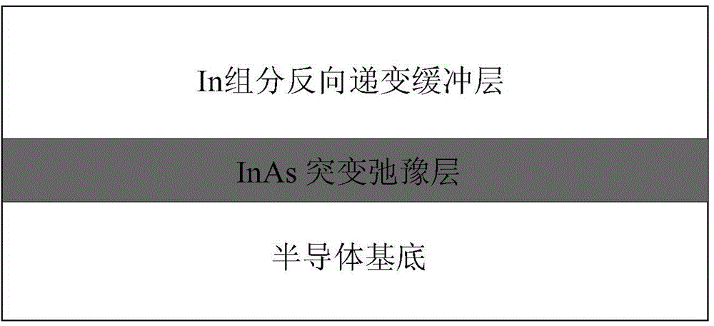
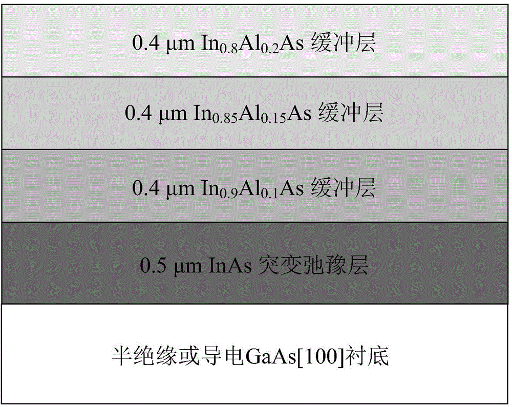
[0021] Suitable for In on GaAs substrate 0.8 Ga 0.2 Abrupt Relaxation Backgrading Buffers for As Detectors

[0022] (1) GaAs single crystal material with [100] crystal orientation is used as the substrate, and InAs with a thickness of about 0.5 μm is first grown on the substrate as a sudden relaxation layer by conventional molecular beam epitaxy method to obtain a relatively flat surface;

[0023] (2) Re-grow a gradient buffer layer with reverse graded In composition, respectively: In with a thickness of 0.4 μm 0.9 al 0.1 As layer, In with a thickness of 0.4 μm 0.85 al 0.15 As layer, In with a thickness of 0.4 μm 0.8 al 0.2 As layer, which is the required suitable In 0.8 Ga 0.2 Abrupt-relaxation reverse-graded buffer layer structure for As detectors.

Embodiment 2

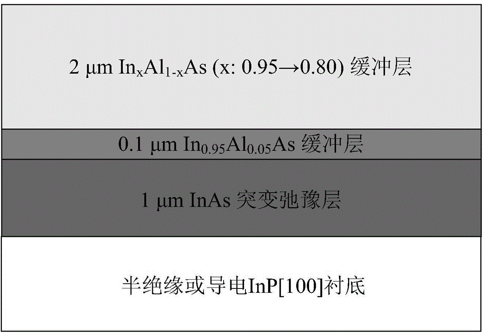
[0025] InP substrate suitable for In 0.8 Ga 0.2 Abrupt Relaxation Backgrading Buffers for As Detectors

[0026] (1) Using the InP single crystal material with [100] crystal orientation as the substrate, and using the conventional molecular beam epitaxy method to first grow InAs with a thickness of about 1 μm on the substrate as a sudden relaxation layer to obtain a relatively flat surface;

[0027] (2) Then grow In with a thickness of 0.1 μm 0.95 al 0.05 AS layer;

[0028] (3) Re-grow In with a thickness of 2 μm and reverse continuous gradient of In composition x al 1-x As buffer layer, where x is reversely graded from 0.95 to 0.8, and its mismatch rate is about 0.67% / μm, this structure is suitable for InP substrate 0.8 Ga 0.2 Abrupt-relaxation reverse-graded buffer layer structure for As detectors.


PUM


Abstract

The invention relates to a mutation relaxation buffer layer for an InGaAs probe with a high In component. An InAs mutation relaxation layer extends on a semiconductor substrate; an arsenide variation structural material of which the In component extends on the InAs mutation relaxation layer and gradually changes in a reversed direction is used as a buffer layer. According to a research method of the InGaAs infrared probe which is arranged on an expandable semiconductor substrate and is provided with the wavelength of more than 1.7 microns, the arsenide variation buffer layer structure of which the In component gradually changes in the reversed direction is adopted, the strain in a larger mismatch InGaAs material can be better released in an expected manner, so that the defect density in an InGaAs absorption layer is reduced, and the device performance is improved; the greater freedom degree is led into a structural designing method of the InGaAs infrared probe with the wavelength of more than 1.7 microns, and the mutation relaxation buffer layer has wide application prospect.

Description

technical field [0001] The invention belongs to the field of semiconductor optoelectronic materials and devices, in particular to a sudden relaxation buffer layer used for high In composition InGaAs detectors. Background technique [0002] Since the InGaAs material is a direct bandgap material with all components, by adjusting the In composition, it can cover the 0.8-3.5 μm band. In addition, InGaAs detectors have the advantages of high sensitivity, fast response, good radiation resistance, and room temperature operation, so InGaAs is an ideal material for short-wave infrared detectors. For example, In with a cut-off wavelength of 1.7 μm at room temperature 0.53 Ga 0.47 As detectors have been widely used in the field of optical communication, and the materials are mainly grown on matching InP substrates. However, as the In composition continues to increase, the mismatch between InGaAs materials and InP substrates will become larger and larger. When the In composition is 8...

Claims


Application Information

Patent Timeline
Patent Type & Authority Applications(China)
IPC IPC(8): H01L31/0304H01L31/101
CPCH01L31/0216H01L31/03046H01L31/101
Inventor 陈星佑顾溢张永刚奚苏萍
Owner 弦海(上海)量子科技有限公司
Why Eureka
Try Eureka