Printed curcuit board and manufacturing method of the same

A technology for printed circuit boards and circuit layers, which is applied in the fields of printed circuit manufacturing, printed circuits, printed circuits, etc., can solve the problems of limited integrated circuit graphics, prevent warping or distortion, reduce preparation costs, and increase integration Effect

Inactive Publication Date: 2015-04-29
SAMSUNG ELECTRO MECHANICS CO LTD
View PDF0 Cites 13 Cited by
  • Summary
  • Abstract
  • Description
  • Claims
  • Application Information

AI Technical Summary

Problems solved by technology

[0015] However, such a conventional method is limited in realizing a thinner and higher-density integrated circuit pattern because it is ultimately a method of additionally adding a portion for preventing warpage of the printed circuit board.

Method used


Image

  • Printed curcuit board and manufacturing method of the same
  • Printed curcuit board and manufacturing method of the same
  • Printed curcuit board and manufacturing method of the same

Examples


preparation example Construction

[0116]A method for preparing a printed circuit board according to an embodiment of the present invention includes: providing a composite material layer having one side and another side, forming a first circuit layer on one side of the composite material layer, and forming a first circuit layer on the composite material layer, respectively. The step of forming a second circuit layer on the other side of the layer, and forming a third circuit layer on the first circuit layer, forming a first insulating layer between the first circuit layer and the third circuit layer , forming a fourth circuit layer on the second circuit layer, and forming a second insulating layer between the second circuit layer and the fourth circuit layer.

[0117] Here, the filler content of the first insulating layer and the filler content of the second insulating layer are formed to be different from each other, and when the remaining copper ratio of the first insulating layer is higher than that of the se...

experiment example

[0137] In this experimental example, in order to observe the warpage occurrence characteristic due to the thermal expansion coefficient of the composite material layer which is a polymer material used in a printed circuit board, the warpage phenomenon was observed while adjusting the amount of the filler.

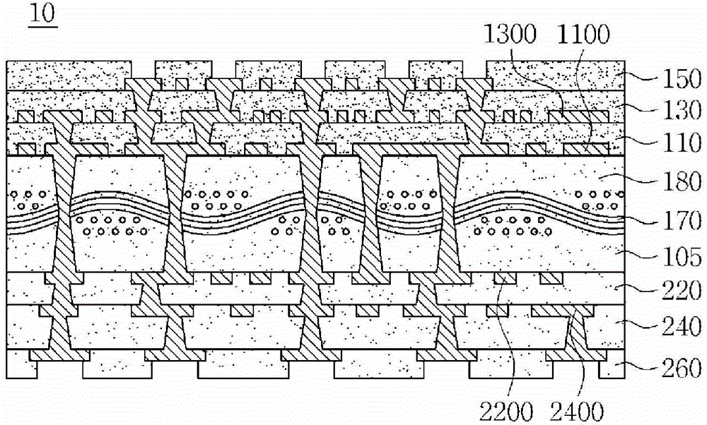
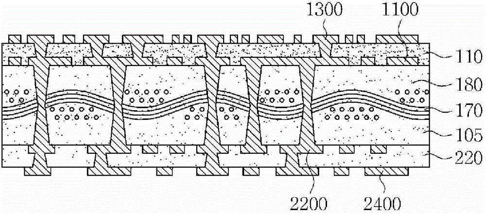
[0138] First of all, for the composition of the printed circuit board, in order to avoid repeated descriptions, cite figure 1 and figure 2 .

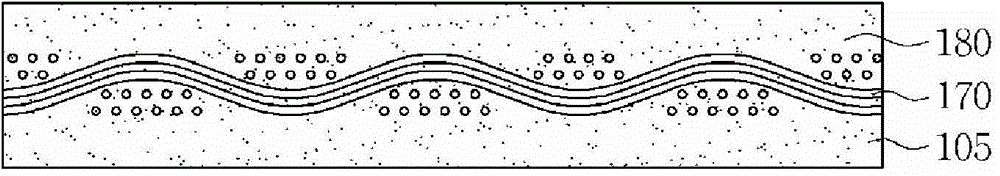
[0139] A composite material layer 105 is formed in the middle of the printed circuit board 10 . Here, the composite material layer 105 is used to increase the modulus of the printed circuit board 10 and is a prepreg containing glass fibers. Such a composite material layer 105 may be a single layer or multiple layers. In addition, circuit layers are formed on both sides of the composite material layer 105, and insulating layers are formed on the circuit layers. In this way, circuit layers and insulating layers are laminated in an...

Embodiment 1

[0149]In Example 1, different from the comparative example, according to the residual copper ratio formed on the composite material layer and the insulating layer, that is, the volume and area of ​​copper, the amount of the filler mixed in the composite material layer and the insulating layer was adjusted and carried out. Add to.

[0150] As shown in Table 1, the residual copper rate of the first circuit layer is 39.8%, and the residual copper rate of the third circuit layer is 43.4%. The first insulating layer existing between the first circuit layer and the third circuit layer The residual copper rate is 83.2%. In addition, the residual copper rate of the second circuit layer was 53.0%, the residual copper rate of the fourth circuit layer was 46.9%, and the residual copper rate of the second insulating layer existing between the second circuit layer and the fourth circuit layer was Formation is 99.9%.

[0151] Here, the filler content was reduced by 20% in the first insula...


PUM


Abstract

The invention relates to a printed curcuit board and a manufacturing method of the same. The printed curcuit board comprises a composite material layer having the other surface corresponding to one surface, a first insulation layer formed on one surface the composite material layer, and a second insulation layer formed on the other surface of the first insulation layer. The coefficients of thermal expansion of the first insulation layer, the second insulation layer and the composite material layer are different. The printed curcuit board selectively adjusts the content of insulation layer filler arranged between copper foil layers, so that the insulation layer with different thermal expansion coefficients are formed, and bad situations such as warping and distortion can be prevented.

Description

technical field [0001] The present invention relates to printed circuit boards and methods for their preparation. Background technique [0002] In recent years, along with the development of electronic devices, weight reduction, thinner board, miniaturization, and higher integration of printed circuit boards are progressing. In order to meet such demands, the structure of printed circuits is further complicated, high-density, and multi-layered. [0003] In addition, due to the shortening of the product cycle, prompt response to customer requests and shortening of the development cycle are required. Under such circumstances, due to the trend of thinner printed circuit boards, the warpage of the substrates delivered to customers has become a core technical problem that should be solved. [0004] In the process of mounting electronic components on such printed wiring boards, thermal expansion and warpage due to heat occur on thinned and multilayered printed wiring boards. He...

Claims


Application Information

Patent Timeline
Patent Type & Authority Applications(China)
IPC IPC(8): H05K1/03H05K3/00H05K3/46B32B15/04
CPCB32B15/08B32B27/20H05K1/0271H05K1/03H05K2201/0141H05K2201/0195H05K2201/0209H05K1/0373H05K3/4626H05K2201/068
Inventor 李根墉李司镛文珍奭
Owner SAMSUNG ELECTRO MECHANICS CO LTD
Why Eureka
Try Eureka