Selective sintering process of printed circuit

A printed circuit, selective technology, applied in the direction of printed circuit, printed circuit manufacturing, electrical components, etc., can solve the problems of poor electrical conductivity, etc., and achieve the effect of high line environment reliability, improved circuit electrical conductivity, and high conductivity

Inactive Publication Date: 2015-04-29
XIAMEN PINGDA TRADING CO LTD
View PDF5 Cites 1 Cited by
  • Summary
  • Abstract
  • Description
  • Claims
  • Application Information

AI Technical Summary

Problems solved by technology

At present, the best conductive metal materials are silver and copper. The sintering of these two conductive material powders requires a higher sintering temperature (greater than 400°C) to obtain better electrical conductivity, which also makes the low-temperature sintering circuit printed on engineering plastics poor electrical conductivity

Method used


Image

  • Selective sintering process of printed circuit

Examples


example 1

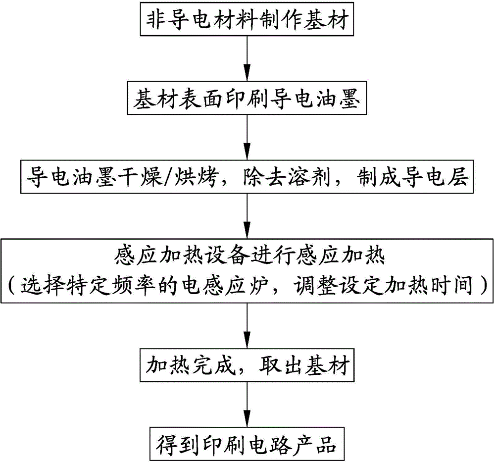
[0031] When the substrate is plastic, conductive ink containing Ag is printed on the plastic surface to form a circuit, and it is first preheated:

[0032] ink material Substrate material heating time Sintering temperature / oven temperature Conductive Silver Ink nylon 30min 60℃ Conductive Silver Ink polycarbonate 3 hours room temperature

[0033] After preheating, sintering by induction heating:

[0034] ink material ink thickness Induction Furnace Frequency / Power heating time The highest temperature of the conductive layer Conductive Silver Ink 8 microns 13.65MHZ / 100W 10S 450℃ Conductive Silver Ink 6 microns 13.65MHz / 80W 15S 500℃

[0035] After sintering, the appearance and size of the substrate did not change. For PC substrates, the conductivity of the sintered metal film layer is 3 to 6 times that of the sintered one hour at 120°C. For some high-temperature nylon substrates, the conductivit...

example 2

[0037] When the base material is wood, brush a layer of conductive nickel ink on the surface of the base material, and the thickness of the ink is 30-40 microns.

[0038] Preheat the sample at 80°C for 20 minutes.

[0039] After preheating, the sample was heated by induction at 2M Hz with a power of 800W for 30S. The instantaneous maximum temperature of the conductive layer is 450°C.

[0040] After sintering, the appearance and size of the substrate remained unchanged, and the electrical conductivity was 4 to 5 times that of the sample sintered at 150°C for 1 hour.

example 3

[0042] Take the eggshell as the base material, and use a syringe to dispense glue to print conductive copper lines on the eggshell. The thickness of the ink is 10-20 microns.

[0043] Let the samples dry naturally for 1 hour.

[0044] The sample is heated at 13.65MHz, 1000W, for 5S. The instantaneous maximum temperature of the conductive layer is 500°C.

[0045] After the sintering was completed, no burning loss was observed in the eggshell inner membrane. The line is on. The electrical conductivity is equivalent to sintering at 150 degrees for 1 hour. However, the burning of local organisms is avoided. Suitable for biological sensing monitoring.


PUM


Abstract

The invention discloses a selective sintering process of a printed circuit. A non-conducting material is selected for manufacturing a base material; the surface of the base material is covered with conducting ink through a printing process; the base material covered with the conducting ink is placed aside so as to remove a solvent in the conducting ink after the conducting ink is dried, or the base material covered with the conducting ink is placed in a baking furnace to be baked at a temperature lower than the softening temperature or denaturation temperature of the base material so as to remove the solvent in the conducting ink; induction heating equipment is used for carrying out induction heating on the base material which has been dried or baked at the low temperature, namely, the base material which has been dried or baked at the low temperature is placed near an induction coil, an electric induction furnace of a specific frequency is selected according to the base material and the conducting ink material, power is adjusted, heating time is set, and heating is carried out; after heating is completed, the printed circuit product can be obtained. By means of the process, selective heating of the printed circuit is achieved, namely, heating is only carried out on the conducting material but not the non-conducting base material, and therefore high-temperature sintering of the printed circuit is achieved, and good electric conductivity is achieved.

Description

technical field [0001] The invention relates to a printing and sintering process, in particular to a selective sintering printed circuit process. Background technique [0002] A printed circuit is an electronic circuit that etches or sensitizes a conductor pattern on an insulating substrate by printing means, and is an electronic circuit that connects electronic components to each other. It has been able to use an automatic plotter to quickly draw the conductor graphics directly on the glass plate to make a plate, and then print it out. Printed circuits make mass production of electronic devices simple and easy, making electronic devices consistent in performance, stable in quality, and compact in structure. Such advances in electronic equipment since the 1950s would not have been possible without printed circuit technology. [0003] In the prior art, when the printed circuit is processed and produced, the conductive paste is printed on the resin substrate, and then the wo...

Claims


Application Information

Patent Timeline
Patent Type & Authority Applications(China)
IPC IPC(8): H05K3/00
Inventor 林顺镇
Owner XIAMEN PINGDA TRADING CO LTD
Why Eureka
Try Eureka