Packaging structure and method of double-sided radiating semiconductor

A packaging structure, double-sided heat dissipation technology, applied in semiconductor devices, semiconductor/solid-state device manufacturing, semiconductor/solid-state device components, etc., can solve problems such as difficulty in ensuring accuracy, overflow of heat sink glue, chip damage, etc., to improve Package quality, the effect of improving the overall heat dissipation performance

Active Publication Date: 2015-05-06
GREAT TEAM BACKEND FOUNDRY (DONGGUAN) LTD
View PDF3 Cites 6 Cited by
  • Summary
  • Abstract
  • Description
  • Claims
  • Application Information

AI Technical Summary

Problems solved by technology

[0002] In semiconductor packaging technology, in order to ensure its heat dissipation, it is necessary to control the overall thickness of the chip and heat sink before packaging. The current thickness control is difficult to ensure its accuracy. If the thickness is too large, the chip will be damaged during the overall injection molding. In severe cases, the chip will be crushed. If the thickness is too thin, there will be glue overflow on the upper surface of the heat sink during the overall injection molding, which will affect the appearance and heat dissipation performance.

Method used


Image

  • Packaging structure and method of double-sided radiating semiconductor
  • Packaging structure and method of double-sided radiating semiconductor

Examples


Embodiment 1

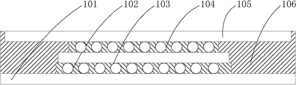
[0030] figure 1 It is a package structure diagram of a double-sided heat dissipation semiconductor provided by the first embodiment of the present invention. Such as figure 1 As shown, the double-sided heat dissipation semiconductor package structure includes:

[0031] The lead frame 101 includes a chip holder, inner leads, and outer leads.

[0032] The first bonding material 102 is located on the chip holder.

[0033] The chip 103 is located on the first bonding material 102.

[0034] The second bonding material 104 is located on the chip 103.

[0035] The heat sink 105 is located on the second bonding material 104.

[0036] Colloid 106, the colloid 106 covers the lead frame 101, the chip 103 and the heat sink 105, and the bottom surface of the chip holder and the top surface of the heat sink 105 leak out of the colloid;

[0037] The first bonding material 102 and the second bonding material 104 contain high temperature resistant equal diameter balls.

[0038] Wherein, the first bonding ...

Embodiment 2

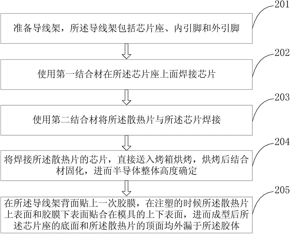
[0044] figure 2 It is a flowchart of a method for packaging a double-sided heat dissipation semiconductor according to the second embodiment of the present invention. Such as figure 2 As shown, the packaging method of the double-sided heat dissipation semiconductor includes:

[0045] Step 201: Prepare a lead frame, which includes a chip holder, inner leads, and outer leads;

[0046] Step 202: Use the first bonding material to solder chips on the chip holder;

[0047] Step 203: Use a second bonding material to weld the heat sink to the chip;

[0048] Step 204: Send the chip welded to the heat sink directly into the oven for baking, and the bonding material is solidified after baking, so that the overall height of the semiconductor is determined;

[0049] Step 205: Paste an adhesive film on the back of the lead frame to perform clamping and injection molding;

[0050] Wherein, the first binding material and the second binding material in step 202 and step 203 contain high-temperature ...


PUM


Abstract

The invention discloses packaging structure and method of a double-sided radiating semiconductor. The packaging structure of the double-sided radiating semiconductor comprises a lead frame, a first combining material, a chip, a second combining material and a radiating plate which are arranged in a rubber coating by wrapping from bottom to top in a sequence; the first combining material and the second combining material are equipped with high temperature resistant balls with the same diameter. The packaging method of the double-sided radiating semiconductor comprises the steps of preparing the lead frame; welding the chip on the upper surface of a chip seat through the first combining material; welding the radiating plate to the chip through the second combining material; directly drying the lead frame welded with the radiating plate through a drying oven; adhering an one-off adhesive film on the rear surface of the lead frame; the bottom surface of the chip seat and the top surface of the radiating plate expose from the adhesive after forming; the first combining material and the second combining material are equipped with the high temperature resistant balls with the same diameter; the overall thickness of the lead frame, the chip and the radiating plate can be accurately controlled before packaging.

Description

Technical field [0001] The invention relates to the technical field of semiconductor packaging, in particular to a double-sided heat dissipation semiconductor packaging structure and a packaging method thereof. Background technique [0002] In semiconductor packaging technology, in order to ensure its heat dissipation, it is necessary to control the overall thickness of the chip and heat sink before packaging. The current thickness control is difficult to ensure its accuracy. If the thickness is too large, the chip will be damaged during the overall injection molding. In severe cases, the chip will be crushed. If the thickness is too thin, glue will overflow on the upper surface of the heat sink during integral injection molding, which will affect the aesthetics and heat dissipation performance. Summary of the invention [0003] The purpose of the present invention is to provide a double-sided heat dissipation semiconductor packaging structure and packaging method thereof, which c...

Claims


Application Information

Patent Timeline
Patent Type & Authority Applications(China)
IPC IPC(8): H01L23/367H01L23/31H01L23/29H01L21/56
CPCH01L2224/14181
Inventor 曹周敖利波
Owner GREAT TEAM BACKEND FOUNDRY (DONGGUAN) LTD
Why Eureka
Try Eureka