Thin film transistor array substrate, manufacturing method thereof, and liquid crystal display device

A technology of thin film transistors and array substrates, applied in the field of liquid crystal display, can solve the problems of low aperture ratio and penetration rate, small aperture area of ​​liquid crystal display devices, etc. The effect of rate increase

Active Publication Date: 2018-04-20
KUSN INFOVISION OPTOELECTRONICS
View PDF3 Cites 0 Cited by
  • Summary
  • Abstract
  • Description
  • Claims
  • Application Information

AI Technical Summary

Problems solved by technology

[0005] The source electrode 14a in the pixel region of the thin film transistor array substrate 1 manufactured by the above seven photomask process steps needs to be designed to a larger area, and then the first through hole 15a is formed on the first insulating protection layer 15 above the corresponding source electrode 14a It is in contact with the first electrode 16, and the material of the source electrode 14a is an opaque material, which blocks the part of the light-transmitting area in the pixel area of ​​the thin film transistor array substrate 1, so that the opening in the pixel area of ​​the thin film transistor array substrate 1 The area is small, resulting in low aperture ratio and transmittance of liquid crystal display devices

Method used


Image

  • Thin film transistor array substrate, manufacturing method thereof, and liquid crystal display device
  • Thin film transistor array substrate, manufacturing method thereof, and liquid crystal display device
  • Thin film transistor array substrate, manufacturing method thereof, and liquid crystal display device

Examples


Embodiment Construction

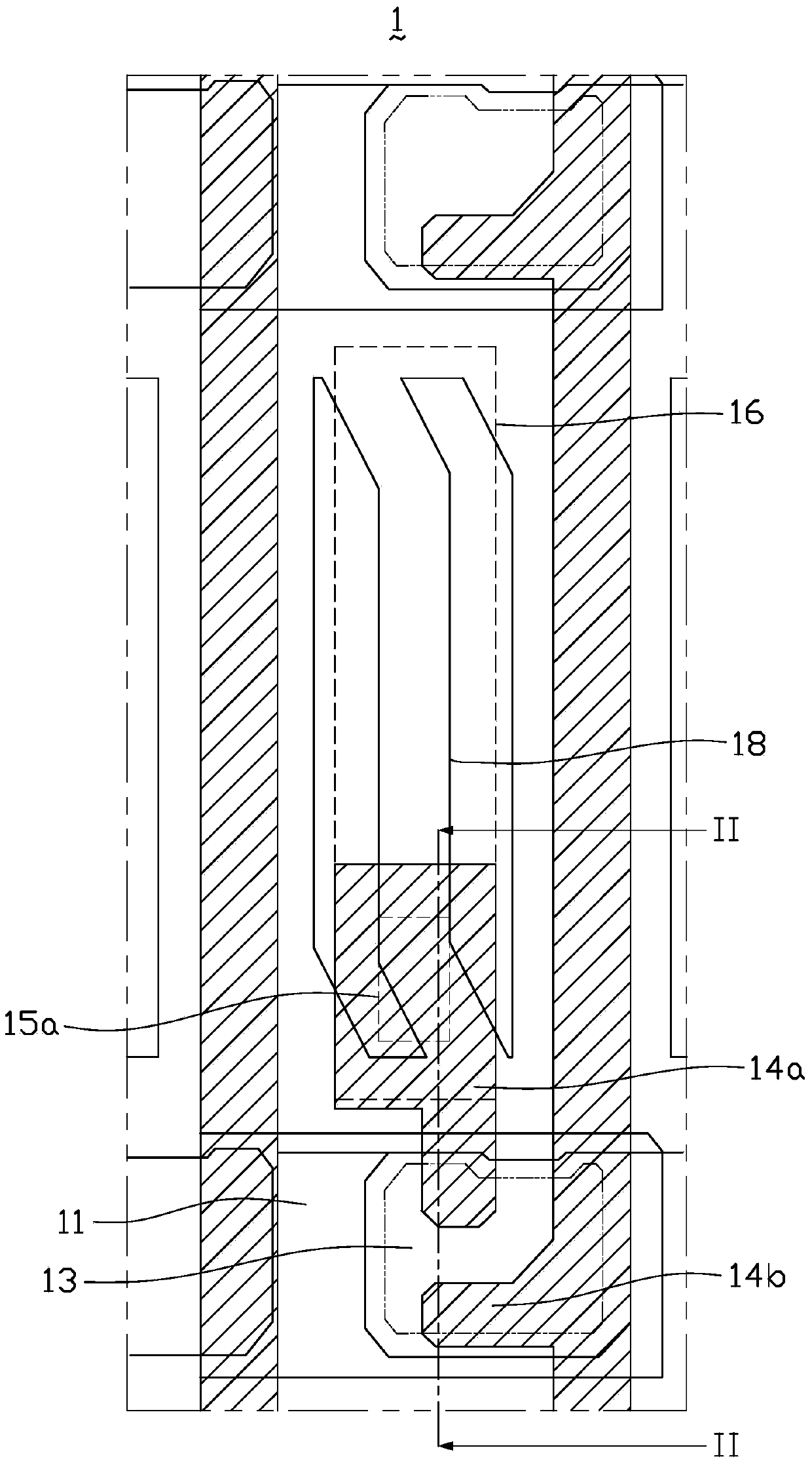
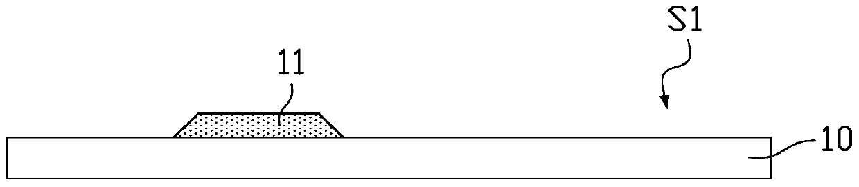
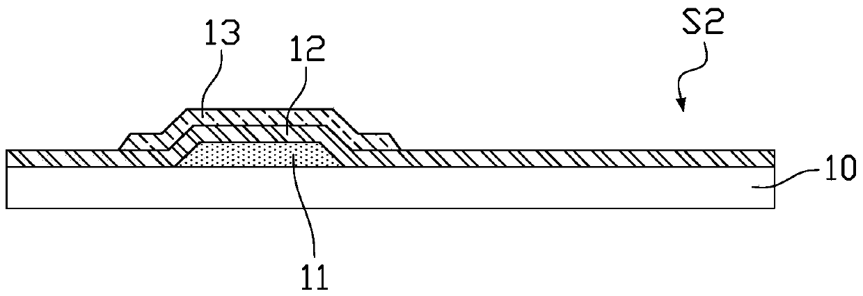
[0029] In order to further explain the technical means and effects of the present invention to achieve the intended purpose of the invention, the thin film transistor array substrate proposed according to the present invention and its manufacturing method, as well as the thin film transistor array substrate with this thin film transistor array are described below in conjunction with the drawings and preferred embodiments. The specific implementation, structure, characteristics and effects thereof of the liquid crystal display device of the substrate are described in detail as follows:

[0030] The aforementioned and other technical contents, features and effects of the present invention will be clearly presented in the following detailed description of preferred embodiments with reference to the drawings. Through the description of specific implementation methods, the technical means and effects of the present invention to achieve the intended purpose can be understood more dee...


PUM


Abstract

The first metal layer of the thin film transistor array substrate is formed on the substrate. The first insulating protection layer is formed on the substrate and covers the first metal layer. A semiconductor layer is formed on the first insulating protection layer. The second metal layer is formed on the first insulating protection layer, including the first source and drain and the second source and drain. The second insulating protection layer is formed on the first insulating protection layer and has a first through hole exposing the first source and drain. The first electrode is formed on the second insulating protective layer. The third metal layer is formed on the second insulating protection layer and the first electrode to fill in the first through hole to be in contact with the first source and drain electrodes, and part of the third metal layer is located on the first electrode and in contact with the first electrode. The third insulating protection layer covers the second insulating protection layer, the first electrode and the third metal layer. The second electrode is formed on the third insulating protection layer. The thin film transistor array substrate has high aperture ratio and transmittance. The invention also relates to a manufacturing method of the thin film transistor array substrate and a liquid crystal display device.

Description

technical field [0001] The invention relates to the technical field of liquid crystal display, and in particular to a thin film transistor array substrate and a manufacturing method thereof, and a liquid crystal display device having the thin film transistor array substrate. Background technique [0002] At present, the display screens of liquid crystal display devices (LCD, Liquid Crystal Display) are getting larger and larger, and in large-size display screens, the higher the number of pixels per inch (PPI, Pixels Per Inch) is, it means that the display The higher the density that the screen can display an image, the more detailed the image will be. The transmittance and aperture ratio of existing high-PPI liquid crystal display devices are still relatively low. In order to improve the transmittance and aperture ratio of liquid crystal display devices, the general method is to use new materials or new technologies such as low temperature polysilicon technology (LTPS, Low ...

Claims


Application Information

Patent Timeline
Patent Type & Authority Patents(China)
IPC IPC(8): H01L27/12H01L21/77G02F1/1343G02F1/1368
Inventor 许传志廖家德李森龙朱晓妮
Owner KUSN INFOVISION OPTOELECTRONICS
Why Eureka
Try Eureka