Solid-state imaging device, manufacturing method of solid-state imaging device, and electronic device

An imaging device and solid-state technology, applied in the field of solid-state imaging devices, can solve the problems of area limitation, hindering the improvement of the sensitivity of photodiodes and memory saturation signal amount photodiodes, and achieve the effect of suppressing aliasing

Active Publication Date: 2020-02-18
SONY CORP
View PDF9 Cites 0 Cited by
  • Summary
  • Abstract
  • Description
  • Claims
  • Application Information

AI Technical Summary

Problems solved by technology

[0003] Therefore, the area where both the photodiode and the memory are provided is limited, which prevents an increase in the saturation signal amount of the photodiode and the memory or an improvement in the sensitivity of the photodiode

Method used


Image

  • Solid-state imaging device, manufacturing method of solid-state imaging device, and electronic device
  • Solid-state imaging device, manufacturing method of solid-state imaging device, and electronic device
  • Solid-state imaging device, manufacturing method of solid-state imaging device, and electronic device

Examples


no. 1 example

[0040] 1. First Embodiment (Example in which a Vertical Transistor is Connected to an End of a Photodiode)

[0041] 2. Second Embodiment (Example in which a Vertical Transistor is Connected to a Central Part of a Photodiode)

no. 3 example

[0042] 3. Third Embodiment (Example in which Photodiodes and Transistors are Connected Through Injection Plugs)

[0043] 4. Fourth Embodiment (Example in which photodiode, memory, and floating diffusion are stacked in three layers)

[0044] 5. Fifth Embodiment (Example of Manufacturing Method When Photodiodes are Firstly Provided on a Substrate)

[0045]6. Sixth Embodiment (Example of Manufacturing Method When Photodiodes Are Lastly Provided on a Substrate)

[0046] 1. The first embodiment

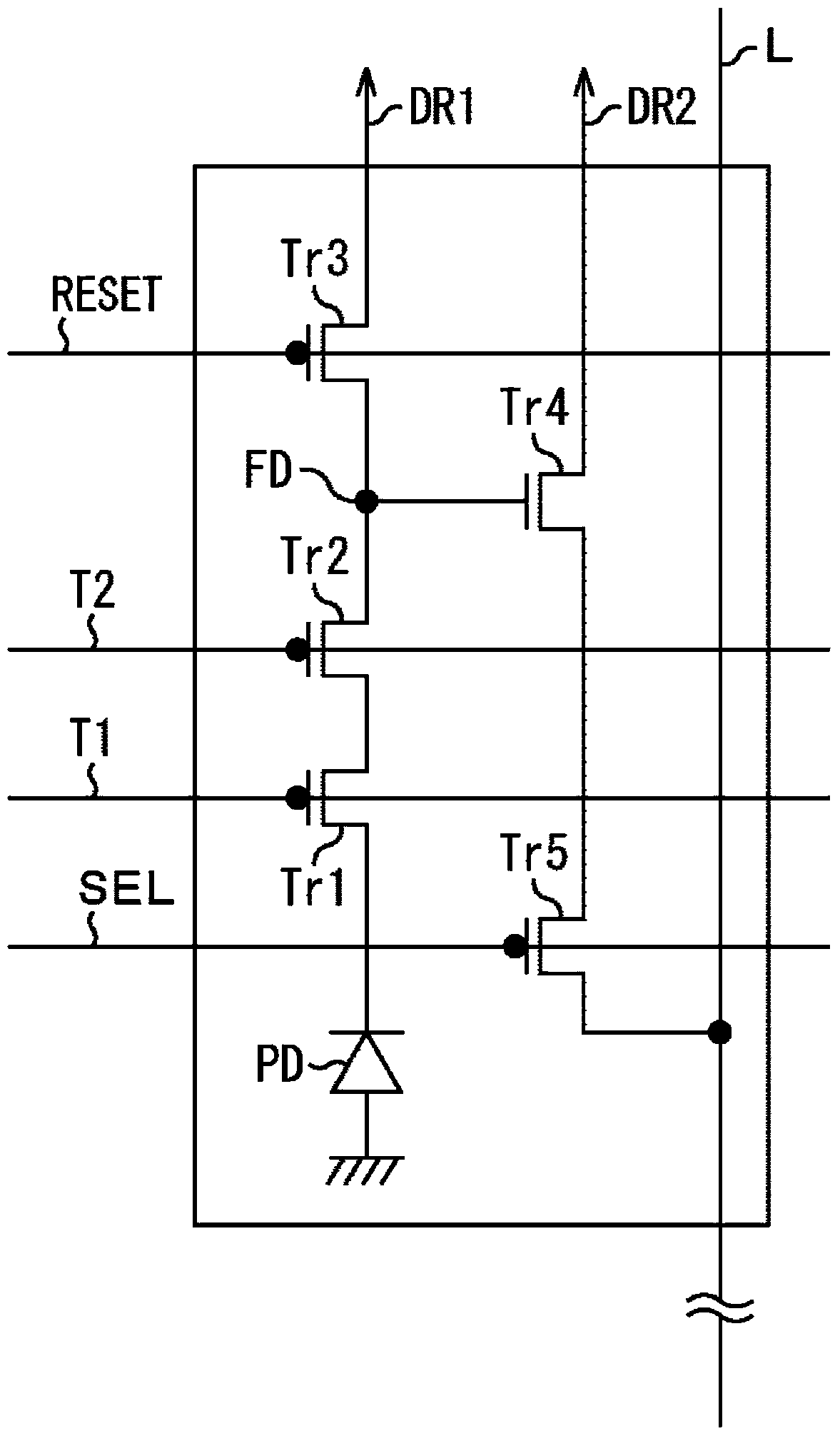
[0047] (Structure of a general solid-state imaging device)

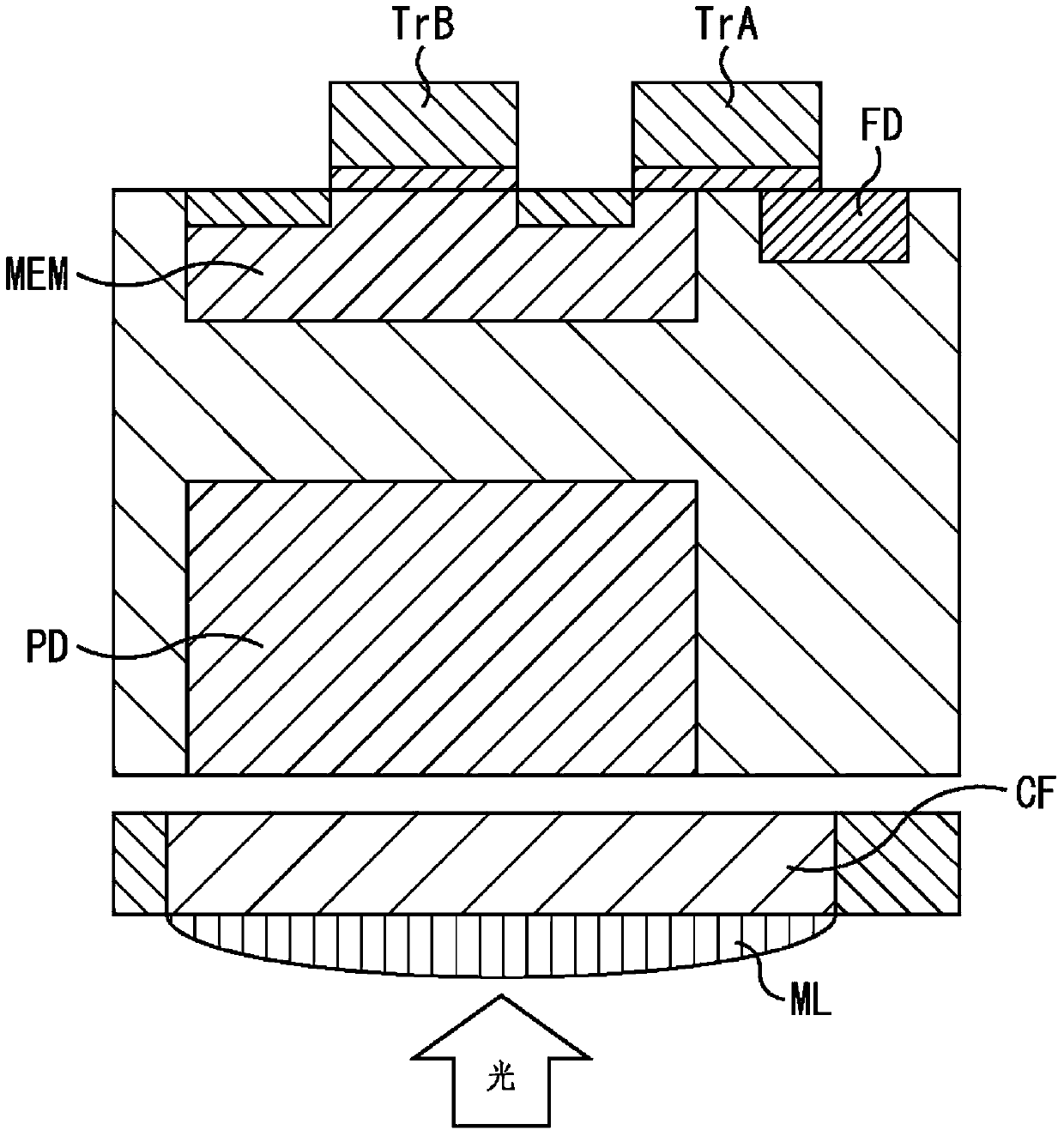
[0048] figure 1 It is a cross-sectional side view of a solid-state imaging device forming a backside-illuminated CMOS (complementary metal oxide semiconductor) image sensor having a global shutter function that has been widely used in the past.

[0049] Backside-illuminated CMOS image sensors with global shutter function include from figure 1 A microlens ML, a color filter CF, a photodiode PD, a memory MEM, a floating diffus...

no. 4 example

[0090] (Fourth structural example of a solid-state imaging device to which an embodiment of the present invention is applied)

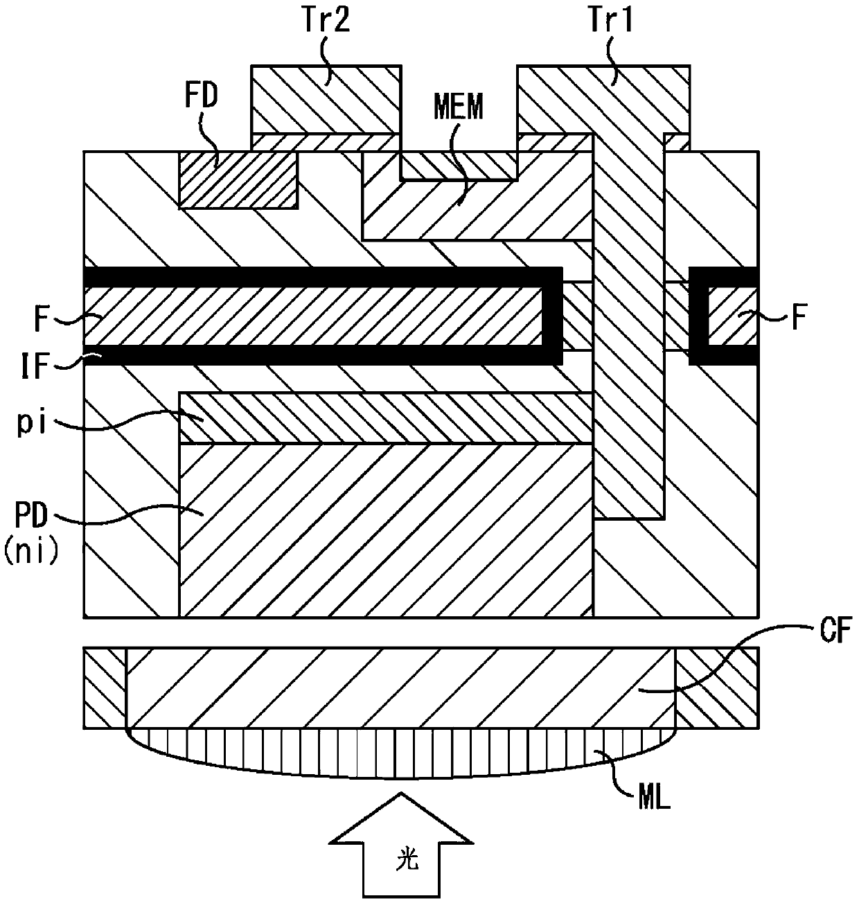
[0091] In the above description, an example in which a two-layer structure including a layer as the upper face of the substrate on which the memory MEM and the floating diffusion FD are formed and a layer as the lower face has been described. In the layers of the photodiode PD, a separation film F is interposed between the upper surface and the lower surface. However, the floating diffusion FD may be laminated on the memory MEM to form a three-layer structure of the floating diffusion FD, the memory MEM, and the photodiode PD.

[0092] Figure 6 A fourth structural example of a solid-state imaging device having a three-layer structure of a floating diffusion FD, a memory MEM, and a photodiode PD formed by laminating the floating diffusion FD on the memory MEM is shown. It should be noted that in Figure 6 Among the solid-state imaging devices, the ...


PUM


Abstract

Provided is a solid-state imaging device including a lamination-type backside illumination CMOS (Complementary Metal Oxide Semiconductor) image sensor having a global shutter function. The solid-state imaging device includes a separation film including one of a light blocking film and a light absorbing film between a memory and a photo diode.

Description

technical field [0001] The present invention relates to a solid-state imaging device, a method for manufacturing a solid-state imaging device, and an electronic device, and more particularly, relates to a method capable of suppressing the generation of aliasing and improving the saturation signal amount of a photodiode (PD) and a memory, and the sensitivity of a photodiode A solid-state imaging device, a manufacturing method of the solid-state imaging device, and an electronic device. Background technique [0002] In a related art backside-illuminated CMOS (complementary metal-oxide-semiconductor) image sensor with a global shutter function, a photodiode (PD) and a memory that temporarily accumulates charges (signals) transferred from the photodiode are provided on the same substrate. flat. [0003] Therefore, the area where both the photodiode and the memory are provided is limited, which prevents an increase in the saturation signal amount of the photodiode and the memory...

Claims


Application Information

Patent Timeline
Patent Type & Authority Patents(China)
IPC IPC(8): H01L27/146H04N5/335
CPCH01L27/1461H01L27/14612H01L27/14614H01L27/14616H01L27/1462H01L27/14623H01L27/14627H01L27/14638H01L27/1464H01L27/14643H01L27/14685H01L27/14687H01L27/14689
Inventor 加藤菜菜子若野寿史
Owner SONY CORP
Why Eureka
Try Eureka