Semiconductor device and method for manufacturing the same
A manufacturing method and semiconductor technology, applied in semiconductor/solid-state device manufacturing, semiconductor devices, electrical components, etc., can solve the problems of different depletion layer extensions and cannot be guaranteed at the same time, and achieve the effect of suppressing the drop in withstand voltage
- Summary
- Abstract
- Description
- Claims
- Application Information
AI Technical Summary
Problems solved by technology
Method used
Image

Examples
Embodiment approach 1
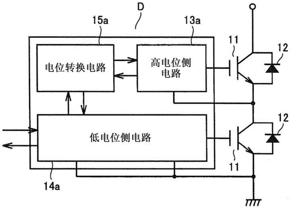
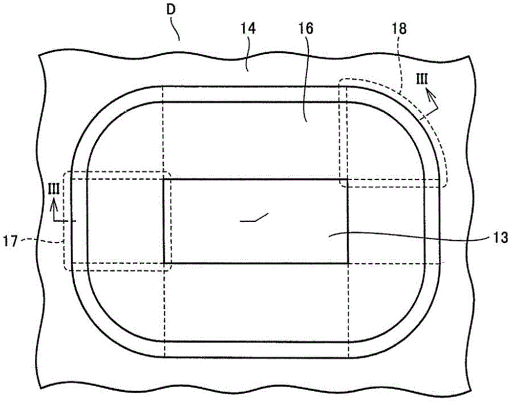
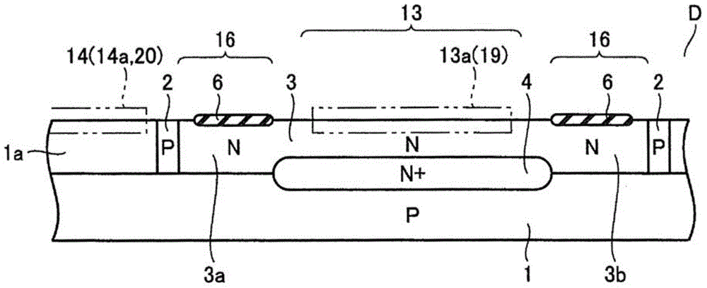
[0067] The semiconductor device D according to Embodiment 1 will be described. like Figure 4 , Figure 5 and Image 6 As shown, for the high voltage isolation region 16, the layout pattern has: a fan-shaped corner 18 with a central angle of about 90°, which is located along the corner pattern of the rectangular high-potential side circuit region 13; and The straight portion 17 is located along the straight line pattern. An N+ type diffusion layer 5 to which a high voltage is applied is formed in the high potential side circuit region 13 .
[0068] The impurity concentration of the N-type diffusion layer 3 b in the corner portion 18 is set to be approximately twice the impurity concentration of the N-type diffusion layer 3 a in the straight portion 17 . Accordingly, the number of atoms of impurities in the N-type diffusion layer 3b and the number of atoms of impurities in the predetermined volume of the N-type diffusion layer 3a become the same number, and it is possible t...
Embodiment approach 2
[0098] Here, a second example of introduction (implantation) distribution of impurities into the high withstand voltage isolation region in the main steps of the manufacturing method of the semiconductor device will be described.
[0099] like Figure 19 and Figure 20 As shown, a resist pattern 43 that exposes the corner portion 18 and the straight portion 17 and covers other regions is formed. Then, using the resist pattern 43 as an implantation mask, the N-type impurity 22a is implanted into the corner portion 18 and the straight portion 17 under the condition that the N-type diffusion layer 3b opposite to the corner portion 18 has an optimum impurity concentration. . Then, the resist pattern 43 is removed.
[0100] Next, if Figure 19 and Figure 21 As shown, a resist pattern 44 covering the corner portion 18 and exposing the straight portion 17 is formed. Then, the P-type impurity 22b is implanted into the straight portion 17 using the resist pattern 44 as an implanta...
Embodiment approach 3
[0104] Here, a third example of the introduction (implantation) distribution of impurities into the high withstand voltage isolation region in the main steps of the manufacturing method of the semiconductor device will be described.
[0105] like Figure 23 and Figure 24 As shown, a resist pattern 45 that exposes the corner portion 18 and the straight portion 17 and covers other regions is formed. Then, using the resist pattern 45 as an implantation mask, the N-type impurity 23a is implanted into the corner portion 18 and the straight portion 17 under the condition that the impurity concentration of the N-type diffusion layer 3a in the straight portion 17 is optimized. . Then, the resist pattern 45 is removed.
[0106] Next, if Figure 23 and Figure 25 As shown, a resist pattern 46 exposing the corner portion 18 and covering the straight portion 17 is formed. Then, N-type impurities 23b are additionally implanted into the corner portion 18 using the resist pattern 46 a...
PUM
 Abstract
Description
Claims
Application Information
 - R&D
- Intellectual Property
- Life Sciences
- Materials
- Tech Scout
- Unparalleled Data Quality
- Higher Quality Content
- 60% Fewer Hallucinations
Browse by: Latest US Patents, China's latest patents, Technical Efficacy Thesaurus, Application Domain, Technology Topic, Popular Technical Reports.
© 2025 PatSnap. All rights reserved.Legal|Privacy policy|Modern Slavery Act Transparency Statement|Sitemap|About US| Contact US: help@patsnap.com