Organic light emission diode and preparation method thereof
An electroluminescent device and electroluminescent technology, which are applied in the fields of electro-solid devices, semiconductor/solid-state device manufacturing, electrical components, etc., and can solve the problems of short service life of OLED devices.
- Summary
- Abstract
- Description
- Claims
- Application Information
AI Technical Summary
Problems solved by technology
Method used
Image
Examples
Embodiment 1
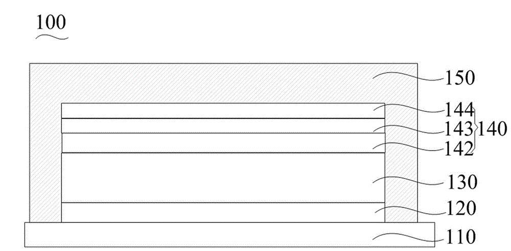
[0059] The structure of the organic electroluminescent device of this embodiment is: PET substrate / ITO / NPB / Ir(MDQ) 2 (acac): CBP(10:100) / Bphen / Al / Li 2 CO 3 : Alq 3 (20:100) / Al / Si 3 N 4 .
[0060] The manufacturing method of the organic electroluminescent device of this embodiment includes the following steps:
[0061] A PET substrate 110 is provided, which is washed and dried for later use.
[0062] A layer of ITO conductive film 120 is prepared on one surface of the PET substrate 110, that is, the anode layer, and is cleaned after completion. The sheet resistance of the anode layer is 5Ω / □.
[0063] A layer of organic electroluminescence unit 130 is prepared on the surface of the ITO conductive film 120 by vacuum evaporation technology:
[0064] The vacuum degree is 1×10 -5 In the Pa vacuum coating system, a hole transport layer with a thickness of 20nm is prepared on the surface of the anode layer, the material used is NPB, and the evaporation rate of NPB is 0.1nm / s;
[0065] The vacuu...
Embodiment 2
[0073] The structure of the organic electroluminescent device of this embodiment is: PET substrate / ITO / MeO-TPD / DCJTB:Alq 3 (5:100) / TPBi / Ag / Cs 2 CO 3 :Bphen(50:100) / Ag / Si 3 N 4 .
[0074] The manufacturing method of the organic electroluminescent device 100 of this embodiment includes the following steps:
[0075] A PET substrate 110 is provided, which is washed and dried for later use.
[0076] A layer of ITO conductive film 120 is prepared on one surface of the PET substrate 110, that is, the anode layer, and is cleaned after completion. The sheet resistance of the anode layer is 100Ω / □.
[0077] A layer of organic electroluminescence unit 130 is prepared on the surface of the ITO conductive film 120 by vacuum evaporation technology:
[0078] The vacuum degree is 1×10 -3 In the Pa vacuum coating system, a hole transport layer is prepared on the surface of the anode layer, the material used is MeO-TPD, the thickness is 60nm, and the evaporation rate is 1nm / s;
[0079] The vacuum degree i...
Embodiment 3
[0087] The structure of the organic electroluminescent device of this embodiment is: PET substrate / ITO / TPD / FIrpic: CBP(15:100) / BCP / Ag-Mg / CsN 3 :TPBi(40:100) / Ag-Mg / Si 3 N 4 .
[0088] The manufacturing method of the organic electroluminescent device 100 of this embodiment includes the following steps:
[0089] A PET substrate 110 is provided, which is washed and dried for later use.
[0090] A layer of ITO conductive film 120 is prepared on one surface of the PET substrate 110, that is, the anode layer, and is cleaned after completion. The sheet resistance of the anode layer is 50Ω / □.
[0091] A layer of organic electroluminescence unit 130 is prepared on the surface of the ITO conductive film 120 by vacuum evaporation technology:
[0092] The vacuum degree is 1×10 -3 In the Pa vacuum coating system, a hole transport layer is prepared on the surface of the anode layer, the material used is TPD, the thickness is 50nm, and the evaporation rate of TPD is 1nm / s;
[0093] The vacuum degree is ...
PUM
 Abstract
Description
Claims
Application Information

