

Transistor forming method
A technology of transistors and contact holes, applied in semiconductor devices, semiconductor/solid-state device manufacturing, electrical components, etc., can solve problems such as silicide damage, and achieve good electrical connection effects
- Summary
- Abstract
- Description
- Claims
- Application Information
AI Technical Summary
Problems solved by technology
Method used
Image

Examples
Embodiment Construction
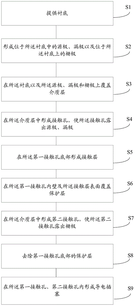
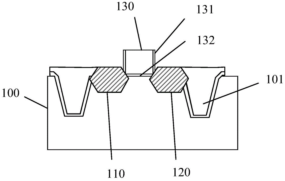
[0037] Aiming at the problem that the silicide contact layer in the contact hole is easily damaged mentioned in the background technology, the formation method of the contact hole in the transistor is analyzed. Before forming the gate contact hole, it is necessary to fill the source-drain contact hole with an organic resist. The etchant layer provides a flat surface for the photolithography of the gate contact hole. In the process of removing the organic resist layer in the source-drain contact hole, it is easy to cause damage to the contact layer at the bottom of the source-drain contact hole. In addition, before filling the conductive layer into the gate contact hole and the source-drain contact hole, it is necessary to clean the inside of the gate contact hole and the source-drain contact hole, and the cleaning agent used for cleaning will also damage the silicide contact layer. .
[0038] A process of forming a protective layer is added between the formation of the gate co...
PUM
| Property | Measurement | Unit |
|---|---|---|
| Thickness | aaaaa | aaaaa |
Abstract
Description
Claims
Application Information