Radio-frequency LDMOS (laterally diffused metal oxide semiconductor) device and process method thereof

A process method and device technology, applied in the field of radio frequency LDMOS devices, can solve problems such as reliability to be improved, and achieve the effects of suppressing snapback effect, improving reliability, and reducing hole injection

Inactive Publication Date: 2015-06-10
SHANGHAI HUAHONG GRACE SEMICON MFG CORP
View PDF5 Cites 0 Cited by
  • Summary
  • Abstract
  • Description
  • Claims
  • Application Information

AI Technical Summary

Problems solved by technology

Although traditional RF LDMOS devices have excellent performance, their reliability needs to be improved

Method used


Image

  • Radio-frequency LDMOS (laterally diffused metal oxide semiconductor) device and process method thereof
  • Radio-frequency LDMOS (laterally diffused metal oxide semiconductor) device and process method thereof
  • Radio-frequency LDMOS (laterally diffused metal oxide semiconductor) device and process method thereof

Examples


Embodiment Construction

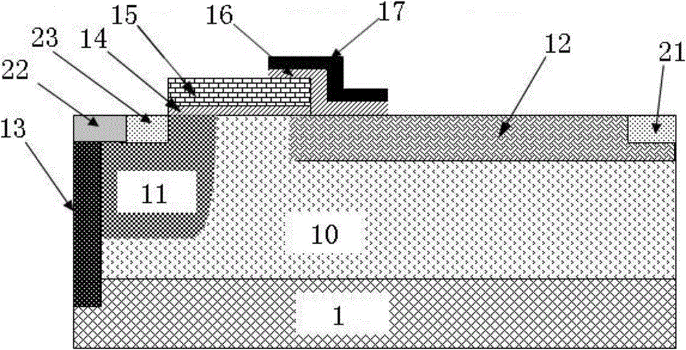
[0025] The radio frequency LDMOS device described in the present invention, such as Figure 5 As shown, there is a P-type epitaxy 10 on a P-type substrate 1, a P-type body region 11 is provided in the P-type epitaxy 10, a heavily doped P-type region 22 and a source region 23 of a radio frequency LDMOS device are located in the P-type In the body region 11; the P-type epitaxy 10 also has a lightly doped drift region 12, and the lightly doped drift region 12 has the drain region 21 of the LDMOS device; the P-type body region 11 and the lightly doped drift The silicon surface between the regions 12 has a gate oxide 14 and a polysilicon gate 15 covering the gate oxide; the polysilicon gate 15 and the lightly doped drift region 12 close to the polysilicon gate cover an oxide layer 16, and the oxide layer 16 There is a Faraday ring 17 on it; on the side of the P-type body region 11 away from the lightly doped drift region 12, there is a tungsten plug 13 that penetrates the epitaxial...


PUM


Abstract

The invention discloses a radio-frequency LDMOS (laterally diffused metal oxide semiconductor) device. A body region and a light-doped drift region are formed in a P-type epitaxy on a P-type substrate, and the epitaxy is provided with a polycrystalline silicon gate and a faraday ring structure. In the P-type epitaxy, a P well is formed below each of the body region and the light-doped drift region, and the P well below the body region and the P well below the light-doped drift region are formed by one-time injection but not connected into a whole. The invention further discloses a process method of the radio-frequency LDMOS device. The process method includes the steps of P well injection, polycrystalline silicon gate formation, body region and source-drain region injection, tungsten plug and faraday ring formation and the like.

Description

technical field [0001] The invention relates to the field of semiconductors, in particular to a radio frequency LDMOS device, and the invention also relates to a process method of the radio frequency LDMOS device. Background technique [0002] RF LDMOS (LDMOS: Laterally Diffused Metal Oxide Semiconductor) device is a new generation of integrated solid-state microwave power semiconductor products formed by the integration of semiconductor integrated circuit technology and microwave electronic technology. It has good linearity, high gain, high withstand voltage, and output power. Large size, good thermal stability, high efficiency, good broadband matching performance, easy to integrate with MOS process, etc., and its price is much lower than that of gallium arsenide devices. It is a very competitive power device and is widely used in GSM , PCS, power amplifiers for W-CDMA base stations, as well as wireless broadcasting and nuclear magnetic resonance. [0003] The structure of...

Claims


Application Information

Patent Timeline
Patent Type & Authority Applications(China)
IPC IPC(8): H01L29/78H01L29/06H01L21/336
CPCH01L29/1083H01L29/402H01L29/4175H01L29/7835
Inventor 慈朋亮石晶胡君李娟娟钱文生刘冬华
Owner SHANGHAI HUAHONG GRACE SEMICON MFG CORP
Why Eureka
Try Eureka