
A semiconductor circuit-based anti-single event effect verification method and system

An anti-single event effect and semiconductor technology, applied in the fields of electrical digital data processing, special data processing applications, instruments, etc., can solve the problems of high cost and long period of verification of anti-radiation devices, and achieve the guarantee of anti-radiation performance and reasonable chip. Area, the effect of controlling the chip area

Active Publication Date: 2018-01-26
SHENZHEN STATE MICROELECTRONICS CO LTD
View PDF4 Cites 0 Cited by
  • Summary
  • Abstract
  • Description
  • Claims
  • Application Information

AI Technical Summary

Problems solved by technology

[0006] The purpose of the embodiments of the present invention is to provide a semiconductor circuit-based anti-single event effect verification method, which aims to solve the current problem of high cost and long cycle for verification of radiation-resistant devices

Method used


Image

  • A semiconductor circuit-based anti-single event effect verification method and system
  • A semiconductor circuit-based anti-single event effect verification method and system
  • A semiconductor circuit-based anti-single event effect verification method and system

Examples


Embodiment Construction

[0036] In order to make the object, technical solution and advantages of the present invention clearer, the present invention will be further described in detail below in conjunction with the accompanying drawings and embodiments. It should be understood that the specific embodiments described here are only used to explain the present invention, not to limit the present invention.

[0037] In the embodiment of the present invention, by loading the heavy particle model on the cascaded CMOS circuit and performing simulation, the sensitive nodes in the circuit can be accurately located, and by performing single-event transient analysis on the cascaded CMOS circuit, the anti-single event effect capability of the circuit can be realized The rapid evaluation of the circuit, and then complete the circuit reinforcement optimization design, while ensuring the product's anti-radiation performance, the chip area is reasonably controlled.

[0038] The realization of the present invention ...


PUM


Abstract

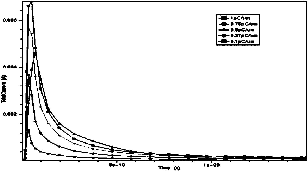
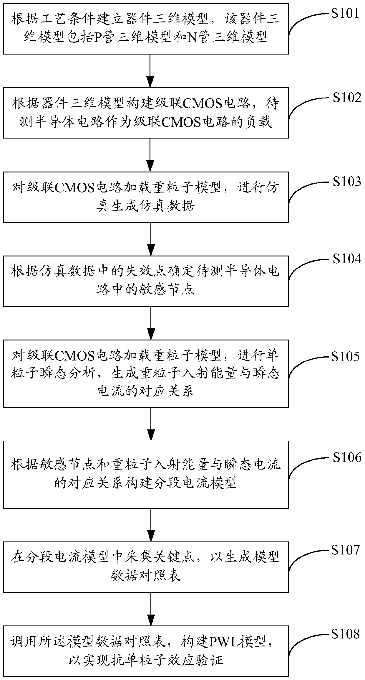
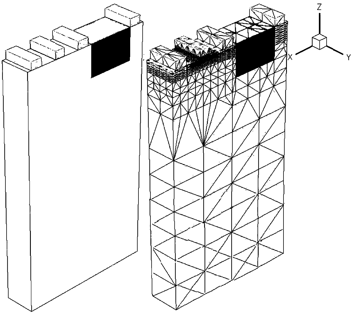
The invention is applicable to the field of semiconductors, and provides a method and system for verifying anti-single event effect based on semiconductor circuits, including: establishing a three-dimensional device model according to process conditions; constructing a cascade circuit according to the three-dimensional model of the device; loading heavy particles on the cascade circuit Model, generate simulation data; determine the sensitive nodes in the circuit according to the simulation data; conduct single-event transient analysis on the cascaded circuit, generate the corresponding relationship between the incident energy of heavy particles and the transient current; construct the segmented current according to the sensitive nodes and the corresponding relationship model; collect key nodes in the segmented current model, and generate a model data comparison table; call the model data comparison table to build a segmented linear current source model. The invention simulates the cascaded circuit after loading the heavy particle model, accurately locates the sensitive nodes in the circuit, and realizes the rapid evaluation of the anti-single event effect ability of the circuit through single-particle transient analysis, ensuring the anti-radiation performance of the product While reasonably controlling the chip area.

Description

technical field [0001] The invention belongs to the field of semiconductors, in particular to a semiconductor circuit-based anti-single event effect verification method and system. Background technique [0002] At present, the rapid development of the aerospace industry urgently needs high-performance radiation-resistant core electronic components, but for a long time, space radiation has caused obvious degradation and failure of the performance of devices and circuits, which seriously restricts the reliability and life of electronic products. It is one of the main radiation effects faced by aerospace applications. [0003] In a radiation environment, when high-energy particles enter the device, a large number of electron-hole pairs are generated along the particle track, and cause the electric field separation in the depletion region to generate charges, which will diffuse to the depletion region and be effectively collected, thus forming transient current. At the same ti...

Claims


Application Information

Patent Timeline
Patent Type & Authority Patents(China)
IPC IPC(8): G06F17/50
Inventor 李孝远陈益冬罗春华邱嘉敏
Owner SHENZHEN STATE MICROELECTRONICS CO LTD
Learn More