Light filter manufacturing method and exposure mask plate

A manufacturing method and a technology of optical filters, which are applied in the direction of optical filters, microlithography exposure equipment, photolithography exposure devices, etc., can solve the problem of increased thickness and cost of optical filters, decreased light transmittance, increased processes and costs and other issues to achieve the effect of improving display performance, increasing flatness, and reducing costs

Inactive Publication Date: 2015-07-01
INESA DISPLAY MATERIALS
View PDF4 Cites 16 Cited by
  • Summary
  • Abstract
  • Description
  • Claims
  • Application Information

AI Technical Summary

Problems solved by technology

[0012] In the prior art, it is necessary to arrange a flat layer 40 on the photoresist layer 30 to make its upper surface relatively flat, so as to reduce the influence of the hor...

Method used


Image

  • Light filter manufacturing method and exposure mask plate
  • Light filter manufacturing method and exposure mask plate
  • Light filter manufacturing method and exposure mask plate

Examples


Embodiment Construction

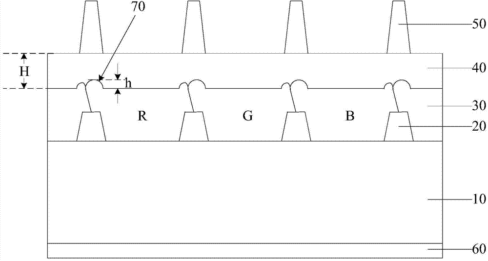
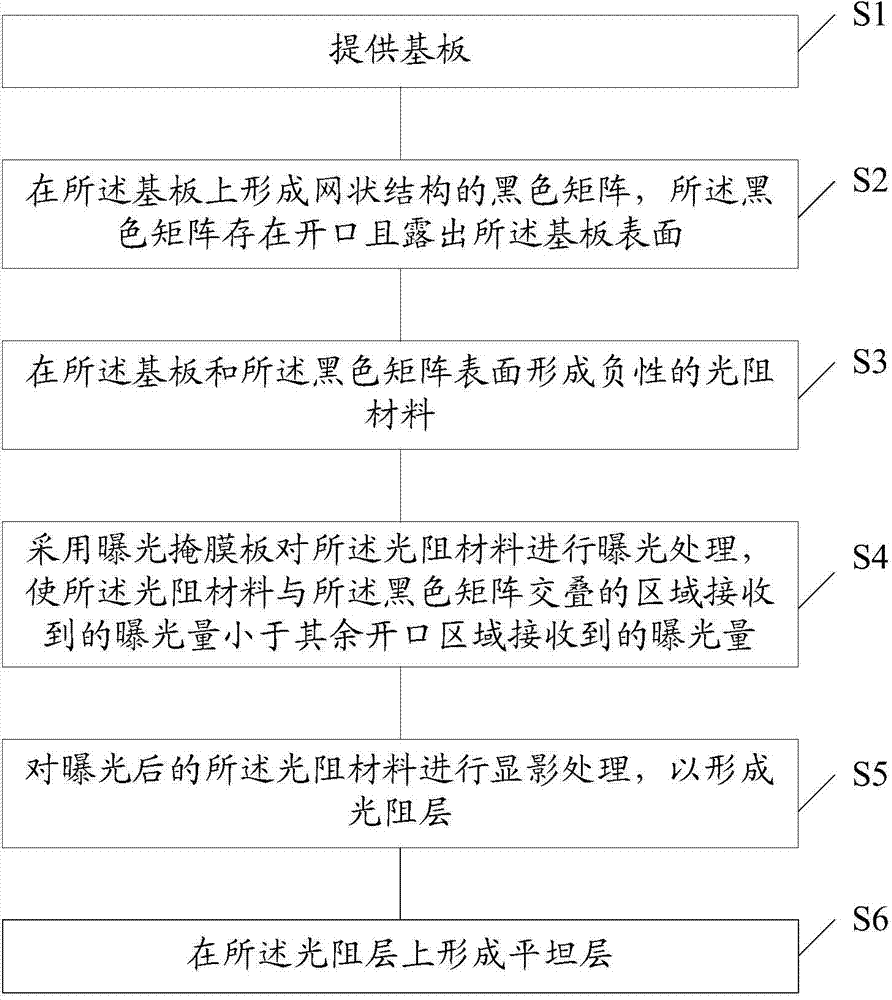
[0039] As mentioned in the background, in the prior art, horns are formed on the edge of the photoresist unit in contact with the black matrix, and the area where the horns are located will make the upper surface of the photoresist layer uneven, which ultimately affects the display performance of the liquid crystal display. Although this technical problem can be solved by forming a flat layer on the photoresist layer, considering that the greater the height of the horns, the worse the flatness of the photoresist layer, the greater the thickness of the flat layer, and the flatness requirements of the flat layer material The higher the value, the higher the cost of the filter, the lower the light transmittance, and the worse the color display effect.

[0040] In view of the above technical problems, the present invention provides a method for manufacturing an optical filter. Since the photoresist layer is a negative photoresist material, the less exposure it receives during the e...


PUM

PropertyMeasurementUnit
Thicknessaaaaaaaaaa
Widthaaaaaaaaaa

Abstract

Provided are a light filter manufacturing method and an exposure mask plate. The light filter manufacturing method comprises the step of providing a substrate; forming a black matrix with a net structure on the substrate, wherein the black matrix is provided with an opening and exposed out of the surface of the substrate; forming a negative photoresist material on the surfaces of the substrate and the black matrix; adopting the exposure mask plate to conduct exposure treatment on the photoresist material and enabling the exposure amount received by a overlapped region of the photoresist material and the black matrix to be smaller than the exposure amount received by the residual open region; conducting developing treatment on the exposed photoresist material to form a light resistance layer. The exposure mask plate is used for the light filter manufacturing method. The exposure mask plate comprises a shading region and an exposure region, wherein multiple protrusion structures are arranged at the edge position in contact with the exposure region in the shading region. The horned portions of the light resistance layer can be decreased or eliminated, the phenomenon that poor liquid crystal deflection caused by too thick horns influences a light filer and the display performance of a liquid crystal display is prevented, and further the cost of light filter can be reduced.

Description

technical field [0001] The invention relates to the technical field of liquid crystal display, in particular to a method for manufacturing an optical filter and an exposure mask. Background technique [0002] At present, liquid crystal display (Liquid Crystal Display, LCD) technology has developed rapidly, and great progress has been made in terms of screen size and display quality. LCD has the characteristics of small size, low power consumption, and no radiation. Occupied a dominant position in the field of flat-panel display. The liquid crystal display panel is the main component of the liquid crystal display, which can be formed by laminating a thin film transistor (Thin Film Transistor, TFT) substrate and another color filter (Color Filter, CF) substrate, and the liquid crystal layer is located between the two substrates . [0003] refer to figure 1 As shown, a kind of optical filter used in liquid crystal display in the prior art can comprise: [0004] glass substr...

Claims


Application Information

Patent Timeline
IPC IPC(8): G02B5/20G02F1/1335G03F7/20
CPCG02B5/223G02F1/133512G02F1/133516G03F1/00
Inventor 张莉唐文静范刚洪陈颖明
Owner INESA DISPLAY MATERIALS
Why Eureka
Try Eureka