Crystal back defect representation method

A technology for crystal back defects and characterization, applied in electrical components, electrical solid-state devices, circuits, etc., can solve the problems of increasing production cost, high price, waste, etc., and achieve the effect of improving production efficiency and simple operation.

Inactive Publication Date: 2015-07-01
SEMICON MFG INT (SHANGHAI) CORP
View PDF8 Cites 11 Cited by
  • Summary
  • Abstract
  • Description
  • Claims
  • Application Information

AI Technical Summary

Problems solved by technology

[0004] 1. Carry out chemical mechanical grinding on the back of the wafer (hereinafter referred to as the crystal back) to meet the shipping standard. However, due to the high price of the existing crystal back grinding equipment, some chip manufacturers often do not set up relevant crystal back grinding equipment, such as Now the most advanced crystal back grinding equipment suitable for 300mm production line, if the relevant grinding equipment is added, the production cost will be greatly increased, and the crystal back grinding process will often bring new wafer defects
[0005] 2. Scrap the wafer, but scrap the entire wafer because of a defect somewhere on the crystal back, which will cause great waste and bring a high cost burden
[0006] However, if there are crystal back defects, it will bring high risks to the subsequent semiconductor flip-chip (Flip-Chip) packaging process. For example, the wafer part at the scratched position is thinner than the wafer part at the unscratched position. During the high temperature process of packaging and testing, the wafer is easy to break at the scratched position, which may further cause integrated circuit leakage or chip failure, so the wafer can only be scrapped

Method used


Image

  • Crystal back defect representation method
  • Crystal back defect representation method
  • Crystal back defect representation method

Examples


Embodiment Construction

[0036] In order to make the above objects, features and advantages of the present invention more comprehensible, specific embodiments of the present invention will be described in detail below in conjunction with the accompanying drawings.

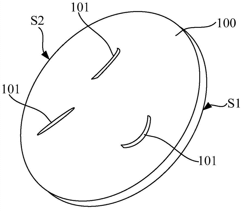
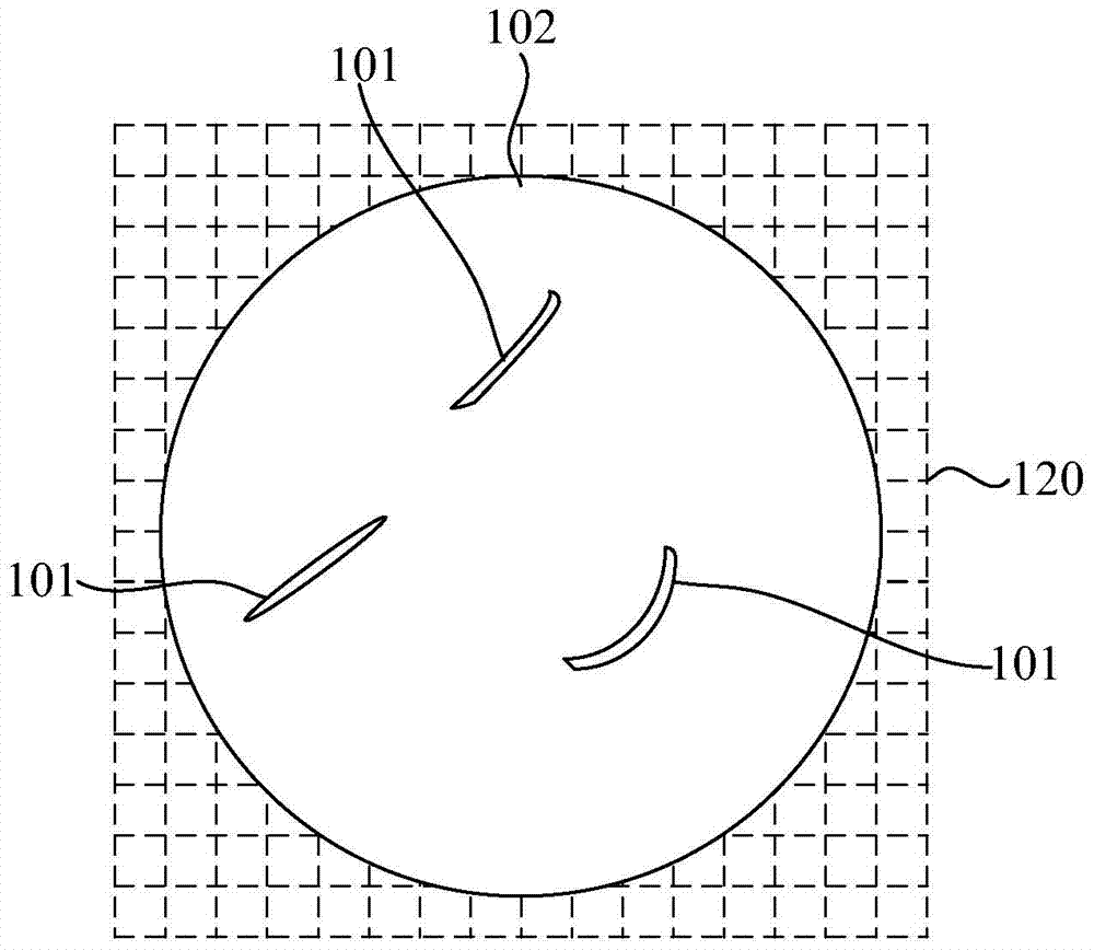
[0037] refer to figure 1 , provide a wafer 100, the wafer 100 includes a wafer front S1 and a wafer back (hereinafter referred to as the crystal back) S2, the crystal back S2 has a crystal back defect 101, and an integrated circuit (not shown in the figure) is formed on the wafer front S1 out).

[0038] It should be pointed out that the crystal back defects 101 refer to macroscopic defects visible to the naked eye such as scratches and chromatic aberrations.

[0039] Wherein, the chromatic aberration refers to that impurities remain on the crystal back S2, and the impurities partially bulge the crystal back S2, making the chromatographic colors of the crystal back S2 inconsistent. Impurities remaining on the crystal back S2 will become ...


PUM


Abstract

A crystal back defect representation method comprises providing a wafer which comprises a wafer front side and a wafer back side, wherein the wafer back side comprise crystal back defects; providing a terminal and establishing a first coordinate system and a second coordinate system at the terminal, wherein the first coordinate system and the second coordinate system are the same coordinate system; inputting a chip distribution diagram of the wafer front side to the terminal and displaying the chip distribution diagram in the first coordinate system to form a chip map; obtaining a crystal back image and displaying the crystal back image in the second coordinate system; forming a defect mark at a position of the crystal back image and recording every defect marks in coordinates in the second coordinate system through the terminal, wherein the position is corresponding to every crystal back defect; marking defect chips on the chip map of the first coordinate system according to the coordinates of every defect mark, wherein every defect chip is aligned to the corresponding crystal back defect. According to the crystal back defect representation method, the crystal back defects are avoided according to the corresponding defect chips in the encapsulation process and accordingly the risk of wafer fractures is reduced and the defect chips obtained through cutting are discarded and accordingly the waste is avoided and the production cost is saved.

Description

technical field [0001] The invention relates to the technical field of semiconductors, in particular to a method for characterizing crystal back defects. Background technique [0002] In the field of semiconductor technology, in the chip manufacturing stage, an integrated circuit is formed on a wafer through the front end process (Front End of Line, FEOL) and the back end process (Back End Of Line, BEOL). Afterwards, the final outgoing quality assurance (OQA) of the finished product needs to be carried out on the wafer formed with the integrated circuit, and the visual inspection work is very heavy and very important. [0003] During the visual inspection process, when defects on the crystal back that exceed the shipping standard, such as serious scratches and chromatic aberrations, are found, there are usually two solutions in the industry: [0004] 1. Carry out chemical mechanical grinding on the back of the wafer (hereinafter referred to as the crystal back) to meet the ...

Claims


Application Information

Patent Timeline
Patent Type & Authority Applications(China)
IPC IPC(8): H01L21/66H01L23/544
CPCH01L22/20H01L22/24
Inventor 刘孜谦谭孝林高燕
Owner SEMICON MFG INT (SHANGHAI) CORP
Why Eureka
Try Eureka