Silicon through hole deep-hole filling process

A technology of through-silicon holes and deep holes, which is applied in the field of microelectronics, can solve problems such as poor film coverage, and achieve the effects of improving film coverage, simple and reasonable process design, and high deposition rate

Active Publication Date: 2015-07-01
BEIJING NAURA MICROELECTRONICS EQUIP CO LTD
View PDF3 Cites 10 Cited by
  • Summary
  • Abstract
  • Description
  • Claims
  • Application Information

AI Technical Summary

Problems solved by technology

[0006] Based on this, it is necessary to provide a TSV deep hole filling process that improves the film coverage of TSV deep hole filling for the problems of poor film coverage when TSVs are deposited.

Method used


Image

  • Silicon through hole deep-hole filling process
  • Silicon through hole deep-hole filling process
  • Silicon through hole deep-hole filling process

Examples


Embodiment Construction

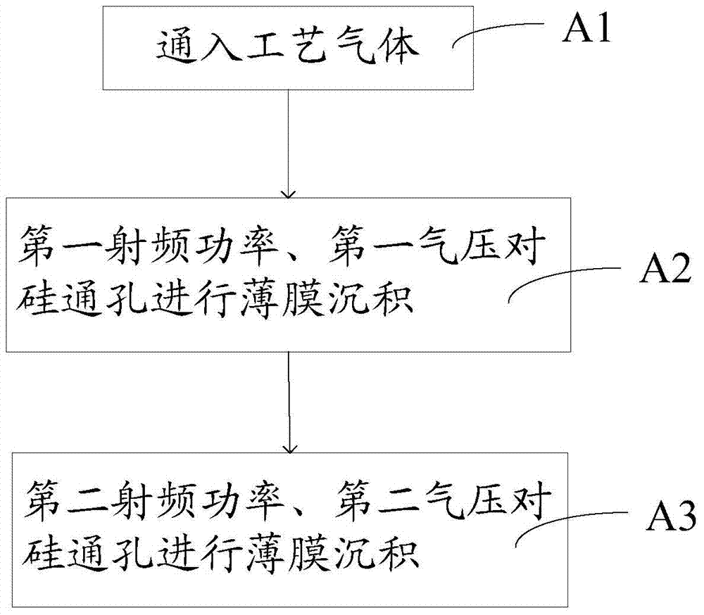
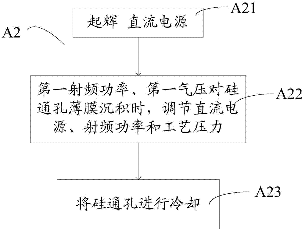
[0045] In order to make the purpose, technical solution and advantages of the present invention clearer, the TSV deep hole filling process of the present invention will be further described in detail through the following embodiments and in conjunction with the accompanying drawings. It should be understood that the specific embodiments described here are only used to explain the present invention, not to limit the present invention.

[0046] Such as figure 1 As shown, the TSV deep hole filling process of the present invention is used to improve the film coverage of TSV deep hole filling, and is applied to magnetron sputtering equipment to make the film coverage inside the TSV uniform and obtain a good Coverage, so that the coverage of the thinnest part of the film is greater than 4%, which can perfectly support the subsequent electroplating process.

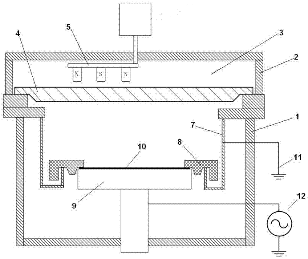
[0047] Such as figure 2 As shown, the magnetron sputtering equipment used in this embodiment is a DC magnetron sputtering e...


PUM


Abstract

The invention provides a silicon through hole deep-hole filling process which is used for improving the film coverage rate during silicon through hole deep-hole filling. The silicon through hole deep-hole filling process comprises the working steps that A1, a process gas is led into a magnetron sputtering device; A2, film deposition is conducted on silicon through holes under the conditions of first radio-frequency power and first air pressure; A3, film deposition is conducted on silicon through holes under the conditions of second radio-frequency power and second air pressure, and repeating the steps A2 and A3 till the film coverage rates in the silicon through holes are even and the required thickness requirement is met. The silicon through hole deep-hole filling process is simple and reasonable in design and adopts the first radio-frequency power and the second radio-frequency power to alternatively perform film deposition, the film coverage rate during silicon through hole deep-hole filling is improved, the process can perfectly support a follow-up electroplating process, and yield is improved.

Description

technical field [0001] The invention relates to the technical field of microelectronics, in particular to a deep hole filling process of through-silicon holes in the microelectronic processing technology. Background technique [0002] Currently, magnetron sputtering, also known as physical vapor deposition (PVD), is a widely used method for depositing metal layers and related materials in the fabrication of integrated circuits. At present, Through Silicon Via (TSV) technology is more and more widely used, which greatly reduces the interconnection delay between chips, and is a key technology for the realization of three-dimensional integration. [0003] In traditional PVD technology, metal atoms and ions are scattered onto the wafer at a certain angle, but for through-silicon vias with high aspect ratio (Aspect Ratio), the scattered metal cannot effectively enter the interior of the via, causing the bottom of the via to be covered by a thin film. The rate is poor. The exist...

Claims


Application Information

Patent Timeline
IPC IPC(8): H01L21/768
CPCC23C14/22C23C14/35H01L21/203H01L21/768H01L21/76877
Inventor 侯珏
Owner BEIJING NAURA MICROELECTRONICS EQUIP CO LTD
Why Eureka
Try Eureka