Perovskite memristor and preparation method thereof

A perovskite and memristor technology, applied in the field of perovskite memristor and its preparation, can solve the problems of poor stability of perovskite and inability to completely solve the instability

Inactive Publication Date: 2021-05-18
HUAZHONG UNIV OF SCI & TECH +1
View PDF3 Cites 2 Cited by
  • Summary
  • Abstract
  • Description
  • Claims
  • Application Information

AI Technical Summary

Problems solved by technology

However, perovskites based on tin or germanium are less stable because Sn2+ is easily oxidized to Sn4+ and G...

Method used


Image

  • Perovskite memristor and preparation method thereof
  • Perovskite memristor and preparation method thereof
  • Perovskite memristor and preparation method thereof

Examples


preparation example Construction

[0035] Another embodiment of the present invention provides a method for preparing the perovskite memristor described above, comprising the following steps:

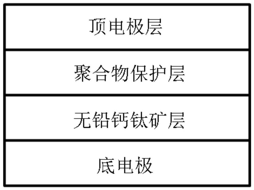
[0036] (1) Spin-coat the lead-free metal halide perovskite precursor solution on the bottom electrode by thermal dynamic spin coating, and then anneal at 100-200°C to form a lead-free perovskite layer on the bottom electrode;

[0037] (2) spin coating a polymer solution on the lead-free perovskite layer, and then annealing at 80°C-100°C to form a polymer protective layer on the lead-free perovskite layer;

[0038] (3) preparing a top electrode on the polymer protective layer by thermal evaporation at an evaporation rate of 0.1-0.3 nm / s, forming a top electrode layer on the polymer protective layer to obtain the perovskite memristor.

[0039] Preferably, the thermal dynamic spin coating method specifically includes: preheating the bottom electrode at 50°C-80°C and keeping it warm, and then putting it on a spin coater for ...

Embodiment 1

[0044] This embodiment provides a method for preparing a perovskite memristor, the method comprising the following steps:

[0045] (1) Pretreatment of the bottom electrode: Use acetone and ethanol to ultrasonically clean the glass (ITO) coated with indium tin oxide for 20 minutes, remove the organic matter on the surface of the ITO, then wash it with deionized water, and finally put it into a UV ozone cleaner Medium treatment for 40 minutes for surface modification.

[0046] (2)AgBiI 4 Preparation of precursor solution: silver iodide and bismuth iodide were mixed and dissolved in DMSO solution at a mass ratio of 1:1, with a concentration of 1M.

[0047] (3) Preparation of lead-free perovskite layer: AgBiI was spin-coated on the pretreated bottom electrode by thermal dynamic spin coating method 4 precursor solution, and then annealed at 100°C to form AgBiI on the bottom electrode 4 perovskite layer. Among them, the bottom electrode is preheated at 60°C, and then placed on a...

Embodiment 2-5

[0054] This example uses the same preparation method as Example 1 to prepare a perovskite memristor. The process parameters of each step in Examples 2-5 are different. The differences between Examples 2-5 and Example 1 are listed in Table 1. show.

[0055] Table 1 Process parameters of steps in the preparation method of perovskite memristor

[0056]

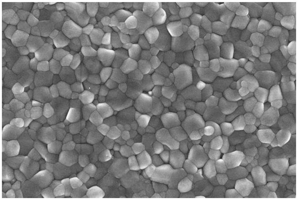
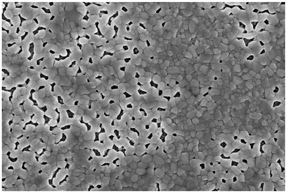
[0057] In the perovskite memristor prepared by Example 2-5, AgBiI 4 The perovskite layers are all dense polygonal nanoparticle structures.


PUM

PropertyMeasurementUnit
Thicknessaaaaaaaaaa
Thicknessaaaaaaaaaa
Thicknessaaaaaaaaaa

Abstract

The invention discloses a perovskite memristor and a preparation method thereof. The perovskite memristor comprises a bottom electrode, a lead-free perovskite layer, a polymer protection layer and a top electrode layer which are arranged from bottom to top, wherein the lead-free perovskite layer is made of lead-free metal halide perovskite, and the lead-free metal halide perovskite is of a compact polygonal nano-particle structure. The method comprises the following steps: spin-coating a lead-free metal halide perovskite precursor solution on a bottom electrode by adopting a thermal dynamic spin-coating method, and performing annealing treatment to form a lead-free perovskite layer on the bottom electrode; spin-coating a polymer solution on the lead-free perovskite layer, annealing, and forming a polymer protection layer on the lead-free perovskite layer; and preparing a top electrode on the polymer protection layer through thermal evaporation, and forming a top electrode layer on the polymer protection layer to obtain the perovskite memristor. According to the invention, the use of toxic lead is avoided, the lead-free perovskite is compact polygonal nanoparticles, the coverage rate is high, and short circuit is prevented.

Description

technical field [0001] The invention belongs to the technical field of memory, and more specifically relates to a perovskite memristor and a preparation method thereof. Background technique [0002] Due to the advantages of fast switching speed, high inheritance density and low power consumption, resistive random access memory has received more and more attention in the fields of memory devices and artificial synapses. Moreover, the simple metal-insulator-metal structure of ReRAM has the potential to achieve high integration density, even overcoming the scaling limitations of current silicon-based flash memory technologies. Flexible electronics have attracted much attention due to their features such as being bendable, foldable, stretchable or wearable, and in these applications, flexible storage devices are urgently needed. So far, although many materials with resistive switching properties have been extensively studied, few reports on flexible memristors have been reporte...

Claims


Application Information

Patent Timeline
IPC IPC(8): H01L45/00
CPCH10N70/801H10N70/20H10N70/881H10N70/026H10N70/011
Inventor 廖广兰叶海波刘智勇刘星月张许宁史铁林汤自荣
Owner HUAZHONG UNIV OF SCI & TECH
Why Eureka
Try Eureka