Remote plasma atomic layer deposition system modulated by variable electric fields

A remote plasma and atomic layer deposition technology, applied in coating, metal material coating process, gaseous chemical plating, etc., can solve the problem of uncontrollable crystal orientation of thin films, and increase adsorption and chemical reaction active sites , Improve the effect of chemical reactivity and film coverage

Inactive Publication Date: 2017-05-31
INST OF MICROELECTRONICS CHINESE ACAD OF SCI
View PDF6 Cites 2 Cited by
  • Summary
  • Abstract
  • Description
  • Claims
  • Application Information

AI Technical Summary

Problems solved by technology

[0004] The embodiment of the present application provides a remote plasma atomic layer deposition system modulated by a variable electric field, which solves the problem that the film deposition rate in the prior art is much lower than the theoretical expectation, and the crystal orientation of the film obtained by atomic layer deposition is random and uncontrollable. The resulting thin film is mostly a polycrystalline thin film with many defects

Method used


Image

  • Remote plasma atomic layer deposition system modulated by variable electric fields
  • Remote plasma atomic layer deposition system modulated by variable electric fields

Examples


Embodiment Construction

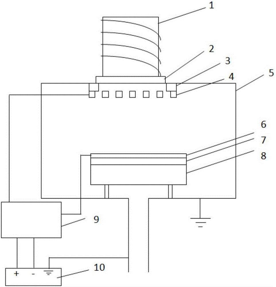
[0020] The embodiment of the present application provides a remote plasma atomic layer deposition system modulated by a variable electric field, which solves the problem that the film deposition rate in the prior art is much lower than the theoretical expectation, and the crystal orientation of the film obtained by atomic layer deposition is random and uncontrollable. The obtained thin film is mostly a problem of a polycrystalline thin film with many defects.

[0021] The technical solution of the embodiment of the present application is to solve the above-mentioned technical problems, and the general idea is as follows:

[0022] A remote plasma atomic layer deposition system with variable electric field modulation. A variable uniform electric field with arbitrarily set size and polarity is introduced into the reaction chamber. The dipole effect on the plasma reaction source and the electric field effect on the plasma reaction source can change the orientation distribution of ...


PUM


Abstract

The invention belongs to the technical field of atomic layer deposition, and discloses a remote plasma atomic layer deposition system modulated by variable electric fields. The remote plasma atomic layer deposition system comprises a cavity, a quartz tube, an insulated ceramic assembly, an upper electrode plate, a lower electrode plate, an insulating pad, a heating plate, an insulating heat-conducting layer, a power supply and a relay. The remote plasma atomic layer deposition system solves the problem that a film is a polycrystal film with more defects as a film deposition rate in the prior art is far lower than a theoretically expected film deposition rate, and crystal orientation of the film obtained by atomic layer deposition is random and uncontrollable. By introducing variable uniform electric fields which can be freely set in size and magnetism into the reaction cavity, adsorption and chemical reaction active sites on the surface of the substrate are increased, and chemical reaction activity and a film coverage rate of a substrate surface are improved, so that the technical effects of realizing laminar growth of atomic layer deposition atomic accuracy resolution and controlling crystallization and doping characteristics of the film are achieved.

Description

technical field [0001] The invention relates to the technical field of atomic layer deposition, in particular to a remote plasma atomic layer deposition system modulated by a variable electric field. Background technique [0002] Atomic layer deposition (ALD) is a method of layer-by-layer growth of single atoms. Compared with chemical deposition, it has inherent advantages. It makes full use of the surface saturation reaction. During the atomic layer deposition process, the chemical reaction of a new layer of atoms It is directly associated with the previous layer, so that only one layer of atoms is deposited for each reaction, with high-precision controllability at the atomic level. ALD technology also has the characteristics of high conformality, and has gradually become an indispensable thin film deposition technology in the field of microelectronics information science. The ALD (PEALD) system with remote plasma source control is added, which increases the activity of th...

Claims


Application Information

Patent Timeline
Patent Type & Authority Applications(China)
IPC IPC(8): C23C16/455C23C16/513
CPCC23C16/45544C23C16/513
Inventor 卢维尔程嵩夏洋李楠
Owner INST OF MICROELECTRONICS CHINESE ACAD OF SCI
Why Eureka
Try Eureka