LED graphic optimized packaging substrate, LED packaging member and manufacture method thereof

A technology for packaging substrates and LED chips, applied in semiconductor devices, electrical components, circuits, etc., can solve the problem of inability to change the light propagation path, and achieve the effects of reliable design indicators, improved light extraction efficiency, and improved extraction probability.

Inactive Publication Date: 2015-07-01
SOUTH CHINA UNIV OF TECH
View PDF9 Cites 2 Cited by
  • Summary
  • Abstract
  • Description
  • Claims
  • Application Information

AI Technical Summary

Problems solved by technology

Integrated COB packaging technology is the mainstream direction of high-power LED development, but the existing COB packaging technology mostly uses planar packaging substrates, which cannot change the p

Method used


Image

  • LED graphic optimized packaging substrate, LED packaging member and manufacture method thereof
  • LED graphic optimized packaging substrate, LED packaging member and manufacture method thereof
  • LED graphic optimized packaging substrate, LED packaging member and manufacture method thereof

Examples


Embodiment 1

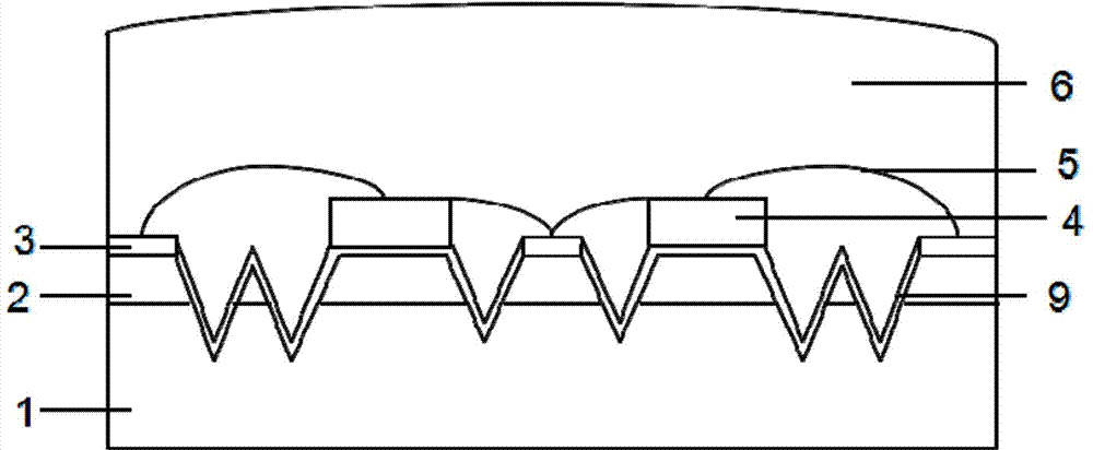
[0038] Such as figure 1 As shown, the LED package of this embodiment includes a package substrate 1 optimized for LED graphics, on which a copper film electrode 3 and an LED chip 4 are arranged, and the positive and negative poles of the copper film electrode 3 and the LED chip 4 pass through The gold wires 5 are connected; the LED chips are packaged on the packaging substrate by COB packaging technology, and the LED chips are covered with an encapsulant 6; the LED chips are arranged periodically and regularly in a rectangular array.

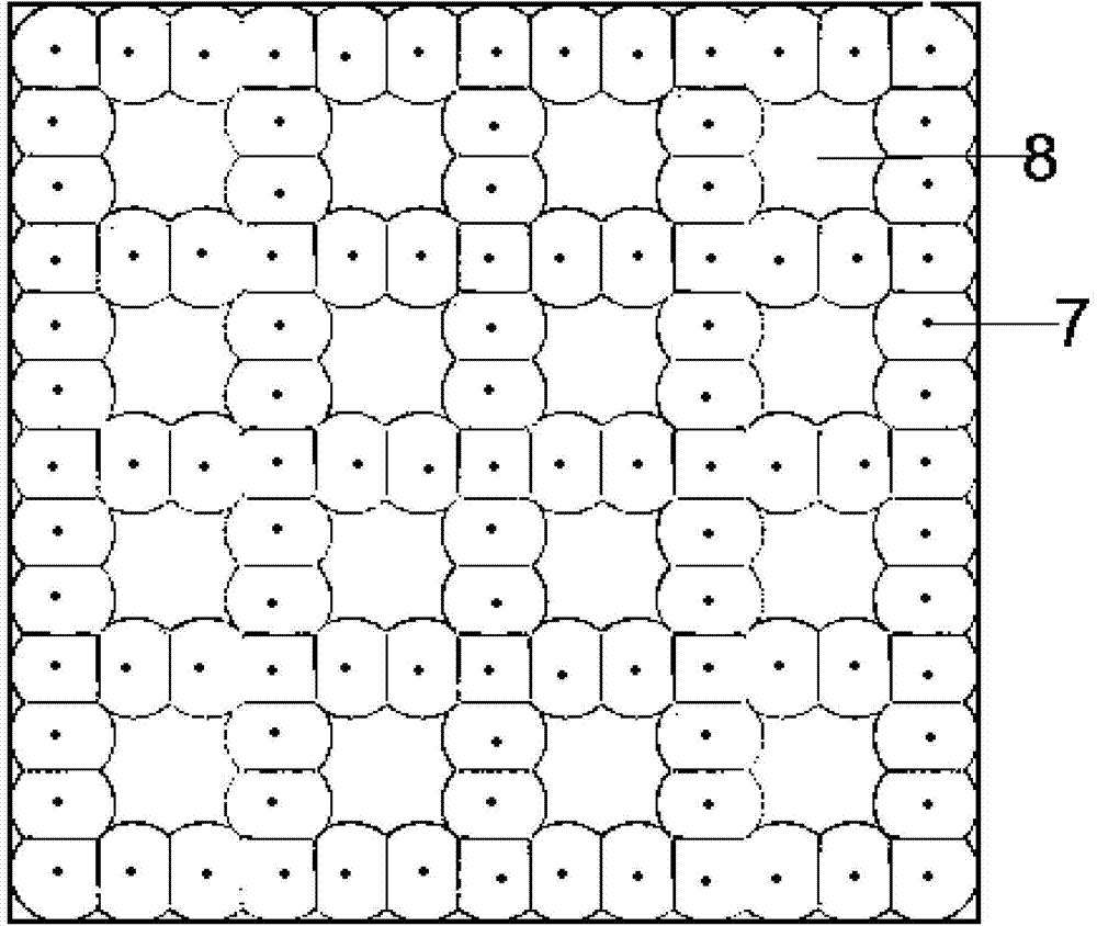
[0039] Such as Figure 2~3 As shown, the LED graphics optimization packaging substrate 1 of the present embodiment is provided with an inverted conical groove pattern, except for the position (LED chip platform 8) reserved for installing LED chips on the packaging substrate, the inverted conical groove 7 adopts a rectangular shape. The array is periodically and regularly arranged; the horizontal surface of the packaging substrate is coated with...

Embodiment 2

[0048] The LED package of this embodiment includes an AlSiC packaging substrate optimized for LED graphics, on which a copper film electrode and an LED chip are arranged, and the positive and negative poles of the copper film electrode and the LED chip are connected by a gold wire; the LED The chip is encapsulated on the packaging substrate by COB packaging technology, and the LED chip is covered with an encapsulant; the LED chips are arranged periodically and regularly in a rectangular array.

[0049] Such as Figure 4 As shown, the LED graphic optimization packaging substrate of this embodiment is provided with inverted conical grooves 7, except for the position (LED chip platform 8) reserved for mounting LED chips on the packaging substrate, the inverted conical grooves are formed in a rectangular array. Periodic and regular arrangement; the horizontal surface of the packaging substrate is coated with a diamond-like carbon insulating layer; the horizontal surface of the pac...


PUM

PropertyMeasurementUnit
Base radiusaaaaaaaaaa
Inclinationaaaaaaaaaa
Center distanceaaaaaaaaaa

Abstract

The invention discloses an LED graphic optimized packaging substrate provided with inverted conical groove patterns. The radius of the bottoms of the inverted conical grooves ranges from 0.3 to 1mm, the incline angle of the inverted conical grooves ranges from 45 to 75 degrees, and the distance between the centers of the inverted conical grooves ranges from 0.5 to 1mm; a silver layer is planted on the horizontal surface and the surfaces of the inverted conical grooves of the packaging substrate. The invention further discloses an LED packaging member with the graphic optimized packaging substrate and a manufacture method thereof. Compared with the prior art, the substrate has the advantages that the direct emitting opportunity is provided for fully reflected light, and the light emitting efficiency is improved by 13.5% around.

Description

technical field [0001] The invention relates to the field of LED packaging, in particular to an LED graphics-optimized packaging substrate, an LED packaging body and a preparation method thereof. Background technique [0002] Compared with traditional light sources, LED has many advantages such as energy saving, environmental protection, and high efficiency, and is recognized as today's green light source. With the continuous development of its technology, the application fields of LED have involved signal indicator lights, automobile headlights, commercial lighting and so on. However, the realization of high-power LEDs still faces the challenge of how to improve light extraction efficiency and achieve a specific optical distribution, and there is room for further improvement. [0003] There are many factors that affect the light extraction efficiency of LEDs, including the crystal quality and number of defects of the GaN epitaxial layer; the particle size of the phosphor p...

Claims


Application Information

Patent Timeline
IPC IPC(8): H01L33/48H01L33/00
CPCH01L33/48H01L33/005H01L33/486H01L33/62
Inventor 李国强杨美娟凌嘉辉张云鹏
Owner SOUTH CHINA UNIV OF TECH
Why Eureka
Try Eureka