Bandgap reference circuit

A reference circuit and reference voltage technology, applied in the direction of adjusting electrical variables, control/regulation systems, instruments, etc., can solve problems such as poor driving ability and easy drop of reference voltage VBG

Active Publication Date: 2015-07-15
SHANGHAI HUAHONG GRACE SEMICON MFG CORP
View PDF5 Cites 10 Cited by
  • Summary
  • Abstract
  • Description
  • Claims
  • Application Information

AI Technical Summary

Problems solved by technology

The driving ability of the existing circuit is poor, when the output terminal of the reference voltage VBG has a large current draw, the reference voltage VBG is easy to drop

Method used


Image

  • Bandgap reference circuit
  • Bandgap reference circuit
  • Bandgap reference circuit

Examples


Embodiment Construction

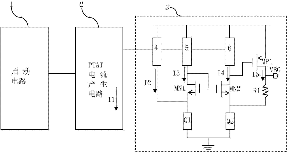
[0039] Such as figure 2 Shown is a schematic structural diagram of the bandgap reference source of the embodiment of the present invention; the bandgap reference circuit of the embodiment of the present invention includes: a start-up circuit 1, a PTAT current generation circuit 2, and an output buffer and reference voltage generation circuit 3.

[0040] The start-up circuit 1 is connected to the PTAT current generating circuit 2 and provides a start-up current when the bandgap reference circuit is turned on.

[0041] The PTAT current generating circuit 2 outputs a first current I 1 , and the first current I 1 is a PTAT current.

[0042] Described output buffering and reference voltage generation circuit 3 comprise:

[0043] The first triode Q1 and the second triode Q2, the first triode Q1 is connected to form a diode structure in which the base and the collector are short-circuited, and the second triode Q2 is connected to form the base and the collector shorted diode struc...


PUM


Abstract

The invention discloses a bandgap reference circuit which comprises a starting circuit, a PTAT (Proportional To Absolute Temperature) current generating circuit and an output buffer and reference voltage generating circuit, wherein the output buffer and reference voltage generating circuit comprises two triodes and three mirror image circuits which form mirror images together with PTAT current, drain electrodes of a first NMOS (N-channel Metal Oxide Semiconductor) tube and a second NMOS tube are respectively connected with the second mirror image circuit and the third mirror image circuit, and a grid electrode and the drain electrode of the first NMOS tube are connected with a grid electrode of the second NMOS tube; the first and second triodes are respectively connected between source electrodes of the first and second NMOS tubes and the ground, and the first mirror image circuit is connected with the source electrode of the first NMOS tube; an output path comprises a first PMOS (P-channel Metal Oxide Semiconductor) tube and a first resistor, a grid electrode of the first PMOS tube is connected with the drain electrode of the second NMOS tube, the first resistor is connected between a drain electrode of the first PMOS tube and the source electrode of the second NMOS tube, and reference voltage is output by the drain electrode of the first PMOS According to the bandgap reference circuit, the driving capability of an output end can be increased, and a temperature coefficient can be improved.

Description

technical field [0001] The invention relates to a semiconductor integrated circuit, in particular to a bandgap reference circuit. Background technique [0002] Such as figure 1 As shown, it is a schematic structural diagram of an existing bandgap reference source; it includes a starting circuit 101 and a bandgap reference main circuit 102 . The PMOS transistors PM0 and PM1 of the bandgap reference main circuit 101 form two mirror circuits, and the source potentials of the NMOS transistors NM0 and NM1 are made to be the same through the NMOS transistors NM0 and NM1 connected to the two mirror circuits, and the transistors Q100 and Q101 are also respectively Located on two mirror circuits, the bases and collectors of transistors Q100 and Q101 are connected together to form a diode structure, figure 1 The transistors Q100 and Q101 shown in are both PNP transistors and the emitter area ratio of the transistors Q101 and Q10100 is N:1, where N is greater than 1, so the base emit...

Claims


Application Information

Patent Timeline
Patent Type & Authority Applications(China)
IPC IPC(8): G05F1/56G05F1/567
Inventor 周宁
Owner SHANGHAI HUAHONG GRACE SEMICON MFG CORP
Why Eureka
Try Eureka