Array substrate, manufacturing method thereof and display panel

A technology for array substrates and display panels, applied in semiconductor/solid-state device manufacturing, optics, instruments, etc., can solve problems such as excessive parasitic capacitance and green images, reduce the influence of parasitic capacitance, avoid signal delay, and improve Display quality effects

Active Publication Date: 2015-07-22
BOE TECH GRP CO LTD +1
View PDF3 Cites 13 Cited by
  • Summary
  • Abstract
  • Description
  • Claims
  • Application Information

AI Technical Summary

Problems solved by technology

[0004] Embodiments of the present invention provide an array substrate, a manufacturing method thereof, and a display panel, which solve the problems of excessive parasitic capacitance between the data line and the common electrode layer and the greening of the image in the structure of the existing array substrate, and avoid the occurrence of signal Delay, improve the display quality of the screen of the display device

Method used


Image

  • Array substrate, manufacturing method thereof and display panel
  • Array substrate, manufacturing method thereof and display panel
  • Array substrate, manufacturing method thereof and display panel

Examples


Embodiment Construction

[0040] The following will clearly and completely describe the technical solutions in the embodiments of the present invention with reference to the accompanying drawings in the embodiments of the present invention. Obviously, the described embodiments are only some, not all, embodiments of the present invention. Based on the embodiments of the present invention, all other embodiments obtained by persons of ordinary skill in the art without making creative efforts belong to the protection scope of the present invention.

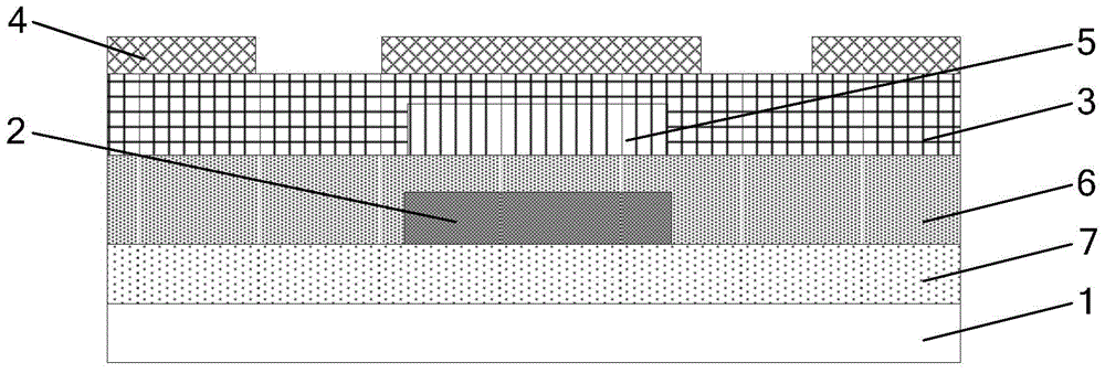
[0041] Embodiments of the present invention provide an array substrate, such as figure 1 As shown in , the array substrate includes a base substrate 1, a data line 2 formed on the base substrate 1, a passivation layer 3 and a common electrode layer 4 formed on the passivation layer 3, and the array substrate also includes a shielding electrode Layer 5 and barrier layer 6, wherein:

[0042] The shielding electrode layer 5 is disposed between the data line 2 an...


PUM


Abstract

The embodiment of the invention provides an array substrate, a manufacturing method thereof and a display panel, and relates to the field of display technologies. The problems that in the structure of an existing array substrate, the size of parasitic capacitors between a data line and a public electrode layer is too large, and pan-green happens on images are solved, signal delay is avoided, and the display quality of pictures of display components is improved. The array substrate comprises a data line, a passivation layer and a public electrode layer, wherein the data line is formed on a substrate body, and the public electrode layer is formed on the passivation layer. The array substrate further comprises a shielding electrode layer and a stopping layer, wherein the shielding electrode layer is arranged between the data line and the passivation layer, the stopping layer is arranged between the data line and the shielding electrode layer which is grounded, and the stopping layer is made of insulating material. The array substrate is applied to the field of display panel manufacturing technologies.

Description

technical field [0001] The present invention relates to the field of display technology, in particular to an array substrate, a manufacturing method thereof, and a display panel. Background technique [0002] The multi-dimensional electric field display mode is a commonly used display mode in liquid crystal display panels. Based on its inherent structural limitations, the process flow of a traditional multi-dimensional electric field display mode display panel is mainly: gate line Gate→active layer Active→data line SD→the first layer of indium tin oxide (Indium tin oxide, referred to as ITO)→ Passivation layer → second layer of ITO, wherein the first layer of ITO is the pixel electrode layer, and the second layer of ITO is the common electrode layer; moreover, the common electrode layer covers the data line. [0003] In this way, since there are other non-conductive film layers between the common electrode layer and the data lines, a large parasitic capacitance will be gene...

Claims


Application Information

Patent Timeline
Patent Type & Authority Applications(China)
IPC IPC(8): G02F1/1362H01L27/12H01L21/77
CPCG02F1/1362G02F1/136286G02F1/136218G02F1/136295H01L27/1214H01L27/1259H01L2021/775G02F1/134309G02F1/134363G02F1/1368G02F1/134372G02F1/13606H01L27/124G02F2201/121G02F2201/123G02F2202/10G02F1/13629H01L21/77
Inventor 王骁
Owner BOE TECH GRP CO LTD
Why Eureka
Try Eureka