
VDMOS (Vertical double-diffused metal oxide semiconductor) and manufacturing method thereof

A manufacturing method and body region technology, which is applied in semiconductor/solid-state device manufacturing, semiconductor devices, electrical components, etc., can solve problems such as channel length and accuracy cannot be guaranteed, and achieve the effect of controllable channel length and accuracy

Active Publication Date: 2015-07-22
FOUNDER MICROELECTRONICS INT
View PDF5 Cites 3 Cited by
  • Summary
  • Abstract
  • Description
  • Claims
  • Application Information

AI Technical Summary

Problems solved by technology

[0009] The embodiment of the present invention provides a VDMOS and its manufacturing method, which is used to solve the problem in the prior art that there is a cumulative deviation in the manufacture of the polysilicon layer and the P-type body region, resulting in a channel formed between the P-type body region and the polysilicon layer. The problem that the length and accuracy cannot be guaranteed

Method used


Image

  • VDMOS (Vertical double-diffused metal oxide semiconductor) and manufacturing method thereof
  • VDMOS (Vertical double-diffused metal oxide semiconductor) and manufacturing method thereof
  • VDMOS (Vertical double-diffused metal oxide semiconductor) and manufacturing method thereof

Examples


Embodiment Construction

[0036] Embodiments of the present invention provide a vertical double-diffused field effect transistor VDMOS and a manufacturing method thereof, which are used to solve the problem in the prior art that there is a cumulative deviation in the manufacture of the polysilicon layer and the P-type body region, which causes the P-type body region to be separated from the polysilicon layer. The length and accuracy of the channel formed between them cannot be guaranteed.

[0037] Embodiments of the present invention will be specifically described below in conjunction with the accompanying drawings.

[0038] The embodiment of the present invention provides a method for fabricating VDMOS, such as Image 6 As shown, the method includes:

[0039] S1: Form an oxide layer on the epitaxial layer, such as Figure 7 shown;

[0040] The thickness of the oxide layer is preferably in the range of about 0.05 μm to 0.15 μm. The growth temperature of the oxide layer is about 1000°C to 1150°C.

...


PUM

PropertyMeasurementUnit
Thicknessaaaaaaaaaa
Thicknessaaaaaaaaaa
Thicknessaaaaaaaaaa

Abstract

The invention discloses a VDMOS (Vertical double-diffused metal oxide semiconductor) and a manufacturing method thereof, so as to solve the problem that the length and precision of a channel formed between a P-type body region and a polycrystalline silicon layer are uncontrollable as cumulative departure exists when the polycrystalline silicon layer and the P-type body region are manufactured in the prior art. The manufacturing method comprises steps: an oxidation layer is formed on an epitaxial layer; an anti-oxidation layer is formed on the oxidation layer, etching is carried out on a preset region of the anti-oxidation layer, and a P-type body region window is formed; three groups of elements are injected to the epitaxial layer via the P-type body region window to form a P-type body region; drive-in of the P-type body region is carried out, and growth of the oxidation layer is continuously carried out in the P-type body region window; the anti-oxidation layer and the oxidation layer are removed, and steps are formed on the surface of the epitaxial layer; a gate oxidation layer is formed on the epitaxial layer after the anti-oxidation layer and the oxidation layer are removed, the surface of the gate oxidation layer has the same shape as that of the epitaxial layer, and the steps on the surface of the epitaxial layer serve as registration Marks to manufacture polycrystalline silicon windows in the gate oxidation layer.

Description

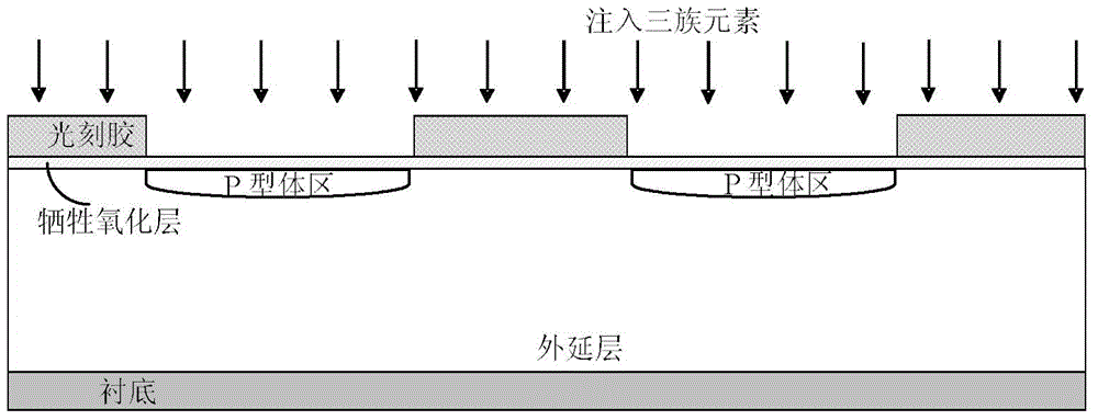
technical field [0001] The invention relates to the technical field of semiconductor chip manufacturing technology, in particular to a VDMOS and a manufacturing method thereof. Background technique [0002] In some special-application planar VDMOS (Vertical double-diffused metal Oxide semiconductor, vertical double-diffused field-effect transistor) manufacturing processes, it is necessary to create a P-type body region (that is, a P-type doped region) before making polysilicon. The length of the channel will be affected by the drive-in of the P-type body region and the registration accuracy of the photolithography of the polysilicon layer. where the channel length as Figure 5 As shown in the dotted circle frame of , the specific steps of making the P-type body region and polysilicon of VDMOS are as follows: [0003] (1), forming a sacrificial oxide layer on the epitaxial layer, coating photoresist on the sacrificial oxide layer, and forming a photoresist window for making ...

Claims


Application Information

Patent Timeline
IPC IPC(8): H01L29/78H01L21/336H01L29/06
CPCH01L29/0684H01L29/66712H01L29/7802
Inventor 马万里刘竹闻正锋
Owner FOUNDER MICROELECTRONICS INT
Learn More