Semiconductor device and method for producing same
A manufacturing method and semiconductor technology, which is applied in semiconductor/solid-state device manufacturing, semiconductor devices, semiconductor/solid-state device components, etc., can solve problems such as gaps and packaging materials that cannot flow in, and achieve the effect of preventing partial discharge
- Summary
- Abstract
- Description
- Claims
- Application Information
AI Technical Summary
Problems solved by technology
Method used
Image
Examples
Embodiment approach 1
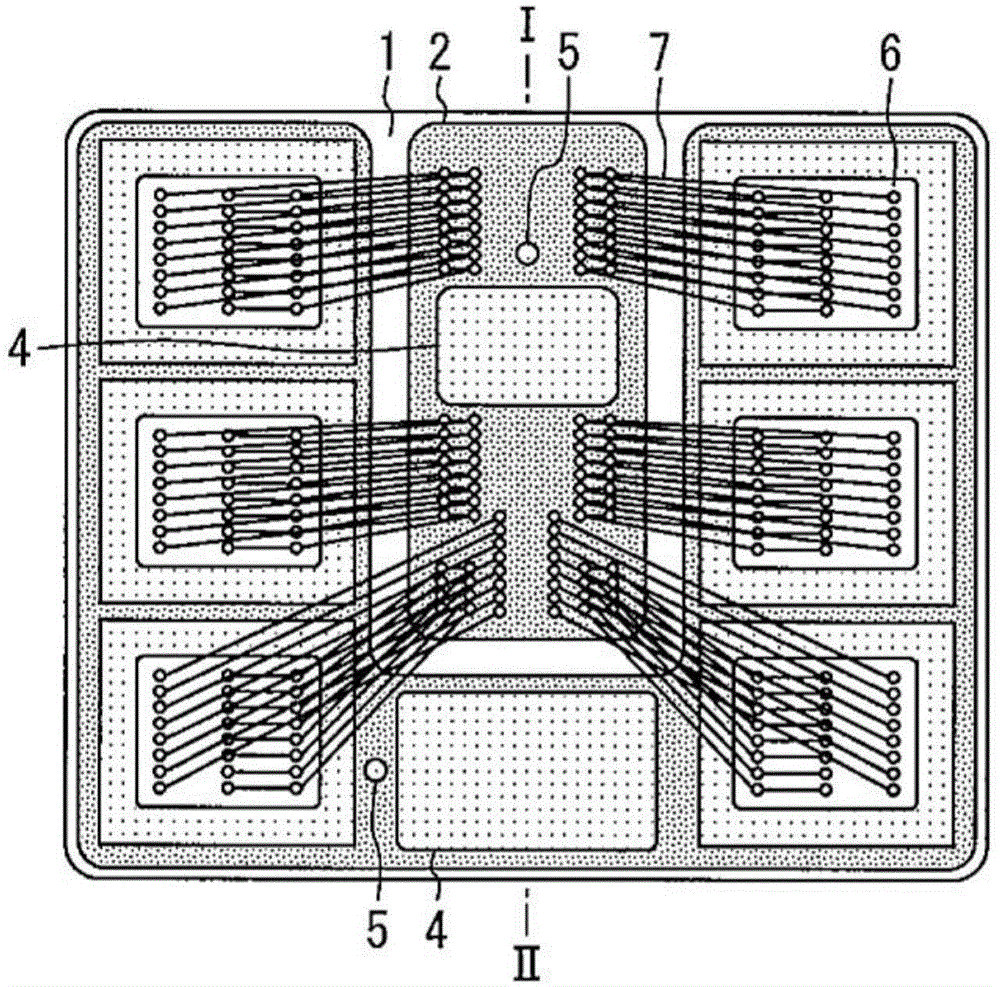
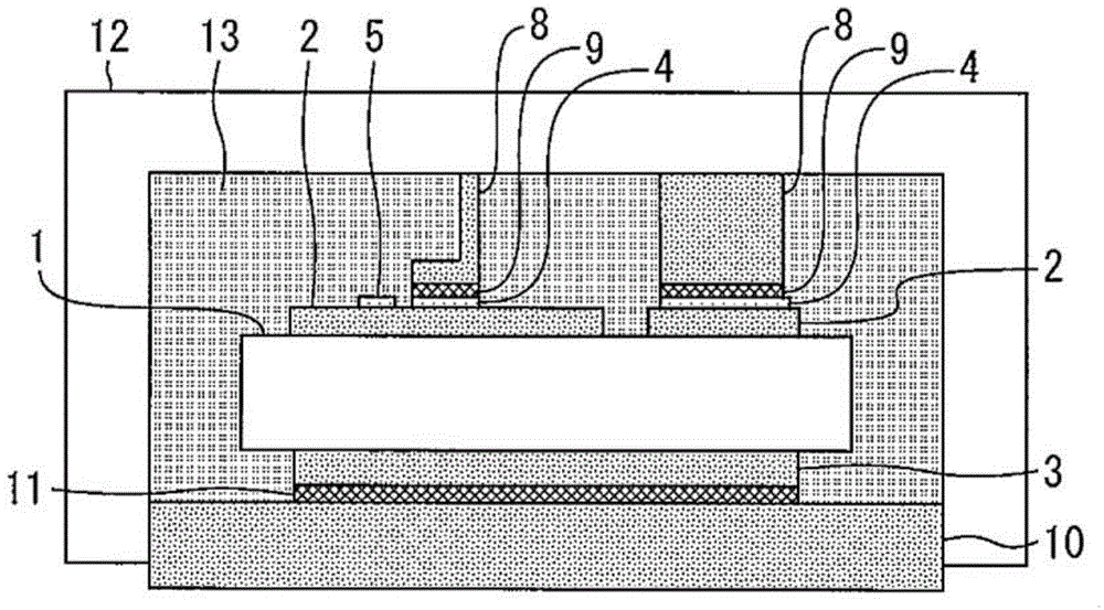
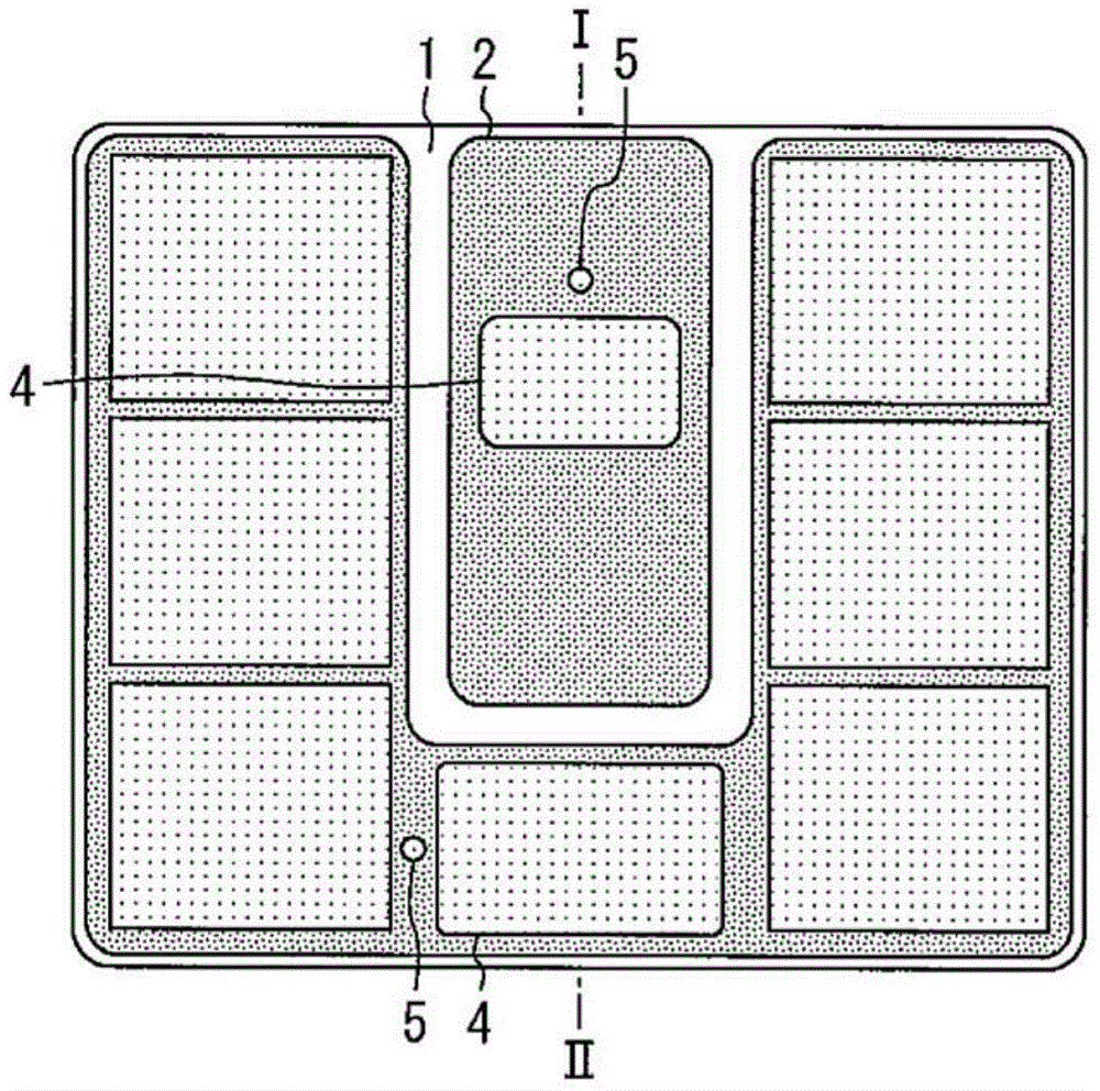
[0027] figure 1 It is a plan view showing the semiconductor device according to Embodiment 1 of the present invention. figure 2 is along figure 1 Sectional view of I-II. The wiring pattern 2 is provided on the upper surface of the insulating substrate 1, and the metal pattern 3 is provided on the lower surface. The soldering portion 4 is provided on the wiring pattern 2 . Ni plating marks 5 are provided on the wiring pattern 2 . The welded part 4 and the mark are made of Ni which is the same material.
[0028] A semiconductor chip 6 is mounted on the insulating substrate 1 . The wire 7 is bonded to the semiconductor chip 6 . Electrode 8 is bonded to welded portion 4 with solder 9 . The base plate 10 is bonded to the metal pattern 3 with solder 11 . These components are entirely covered by a case 12 , and the insulating substrate 1 , semiconductor chip 6 , wires 7 , and electrodes 8 are encapsulated by an encapsulating material 13 .
[0029] Next, a method of manufact...
Embodiment approach 2
[0034] Figure 5 It is a plan view showing the semiconductor device according to Embodiment 2 of the present invention. Image 6 is along Figure 5 Sectional view of I-II. In addition, in Figure 5 In , the semiconductor chip 6 and the wire 7 are omitted.
[0035] Instead of the Ni-plated mark 5 of Embodiment 1, a solder resist mark 15 made of solder resist is arranged on the wiring pattern 2 . The protective film 16 made of solder resist covers the outer periphery of the wiring pattern 2 . The protective film 16 and the solder resist mark 15 are simultaneously formed using a solder resist. The wire 7 is bonded to the semiconductor chip 6 by identifying the position of the insulating substrate 1 by the solder resist mark 15 . The other structures and manufacturing steps are the same as those of Embodiment 1.
[0036] The solder 9 flowing out from the soldered portion 4 does not adhere to the solder resist mark 15 made of solder resist, and thus no voids are generated. ...
Embodiment approach 3
[0038] Figure 7 It is a plan view showing the semiconductor device according to Embodiment 3 of the present invention. Figure 8 is along Figure 7 Sectional view of I-II. In addition, in Figure 7 In , the semiconductor chip 6 and the wire 7 are omitted.
[0039] A protective film 16 made of solder resist is provided on the insulating substrate 1 . This protective film 16 has an opening 17 arranged at the welded portion 4 and an opening 18 arranged outside the welded portion 4 . Electrode 8 is bonded to solder 9 via opening 17 . Then, the wire 7 is bonded to the semiconductor chip 6 by identifying the position of the insulating substrate 1 through the opening 18 . The other structures and manufacturing steps are the same as those of Embodiment 1.
[0040] The solder 9 flowing out from the soldered portion 4 does not adhere to the protective film 16 made of solder resist, and therefore does not reach the opening 18 and does not generate voids. Therefore, occurrence of...
PUM
 Abstract
Description
Claims
Application Information


