A thin film sample preparation method for in situ applied electric field and stress for transmission electron microscopy

A technology of transmission electron microscopy and sample preparation, which is applied in the field of in-situ transmission electron microscopy research on epitaxial thin film materials, and can solve problems such as the inability to provide the space required for the positioning and movement of nanoprobes

Active Publication Date: 2017-11-28
HUBEI UNIV
View PDF5 Cites 0 Cited by
  • Summary
  • Abstract
  • Description
  • Claims
  • Application Information

AI Technical Summary

Problems solved by technology

The thin area prepared by this method is in the center of the copper ring and the single crystal substrate, and the thin film in the thin area is surrounded by the ring and the single crystal substrate, which cannot provide the required positioning and movement of the nanoprobe loaded with mechanical stress and electrical signals. space

Method used


Image

  • A thin film sample preparation method for in situ applied electric field and stress for transmission electron microscopy
  • A thin film sample preparation method for in situ applied electric field and stress for transmission electron microscopy
  • A thin film sample preparation method for in situ applied electric field and stress for transmission electron microscopy

Examples


Embodiment Construction

[0024] The present invention will be further described below in conjunction with the accompanying drawings and embodiments.

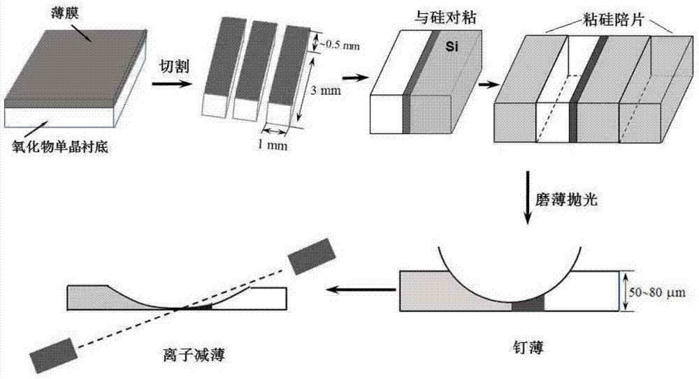
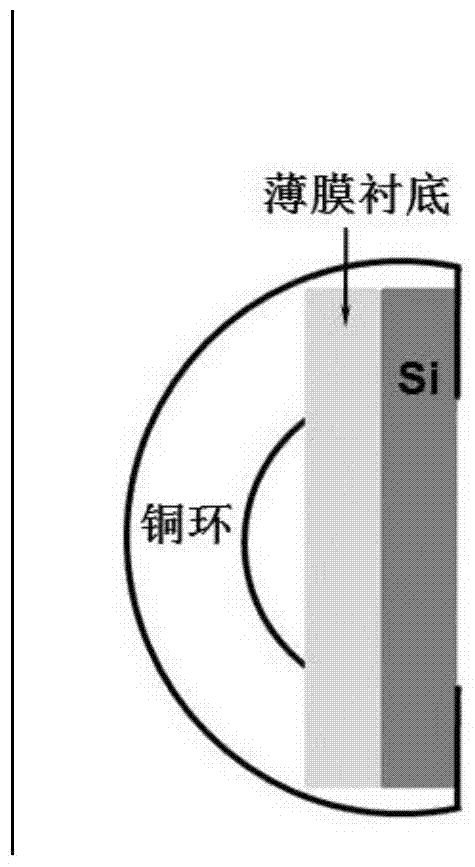
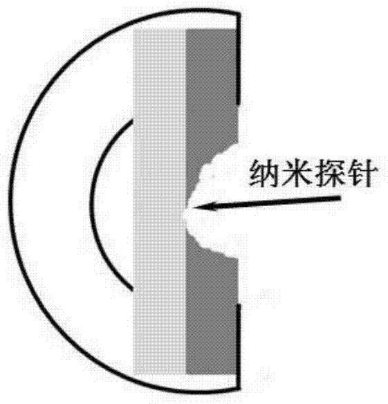
[0025] Such as figure 1 As shown, this embodiment provides a method for preparing thin film cross-section samples for in-situ application of electric field and stress in transmission electron microscopy. Using the characteristic that the ion thinning rate of Si material is much higher than that of single crystal oxide, Si sheets and thin film materials are selected For bonding, the Si sheet is knocked off by argon ions before the film and the substrate, so that the epitaxial film is exposed, which is beneficial to apply the electric field and stress through the probe. It specifically includes the following steps:

[0026] (1) Film cutting and Si one-side bonding

[0027] Will grow the BiFeO 3 thin film GdScO 3 Oxide single crystals and single crystal Si are cut into strips with a size of 3mm×1mm×0.5mm. Si bar polished surface and BiFeO 3 The membr...


PUM

PropertyMeasurementUnit
diameteraaaaaaaaaa
thicknessaaaaaaaaaa

Abstract

The invention proposes a thin film sample preparation method for in situ application of electric field and stress for a transmission electron microscope. The steps are (1) cutting the thin film to be tested and the single crystal Si substrate into strips of 3mm×1mm×0.5mm, and then sticking the film surface of the thin film strip to the polished surface of the Si strip; (2) cutting the thickness of the thin film strip Both sides are mechanically ground and polished, (3) use a nail thinner for nail thinning, (4) bond the half copper ring, (5) use an ion thinner for ion thinning, set the ion gun voltage to 4kV, and set the angle Set at 6°, thinning for 20-40 minutes; change the angle to 4°, thinning for 15-30 minutes, and finally use a voltage of 3kV, and polish at an angle of 3° for 3 minutes to obtain a large area of ​​perforation at the bonding seam, and a large area of ​​the bonding Si sheet. The area is bombarded by ions, exposing the film, which can be applied with electric field and stress by probe, and there is a large thin area suitable for electron microscope observation at the edge.

Description

technical field [0001] The invention belongs to the technical field of in-situ transmission electron microscopy research on epitaxial thin film materials, and specifically relates to a preparation method and application of a transmission electron microscope sample suitable for in-situ stress and electric field applied to epitaxial thin films. Background technique [0002] The in-situ transmission electron microscopy technology not only has the high-resolution ability of the transmission electron microscope, but also can observe the structural changes of the material in real time at the atomic scale in situ, and can also apply external fields (such as stress, electric field and optical signal, etc.) simultaneously. It is the core of modern material research. It is an important technical means, which can be widely used in the research of the growth or force deformation of nanomaterials, the influence of electricity and magnetic field on the structure and performance of material...

Claims


Application Information

Patent Timeline
Patent Type & Authority Patents(China)
IPC IPC(8): G01N1/28G01N1/32
Inventor 祁亚军章天金梁坤周鹏梅之恒叶昂
Owner HUBEI UNIV
Why Eureka
Try Eureka