Display panel, method and device for debugging flicker, and display device

A technology for display panels and substrates, applied in measuring devices, static indicators, optics, etc., can solve the problems of screen flicker in the display panel and easy to be detected by the human eye, reduce the voltage change value, and improve the screen flicker phenomenon. Effect

Active Publication Date: 2015-08-12
BOE TECH GRP CO LTD
View PDF5 Cites 11 Cited by
  • Summary
  • Abstract
  • Description
  • Claims
  • Application Information

AI Technical Summary

Problems solved by technology

[0007] To sum up, in the prior art, when the pixel electrode drives the liquid crystal to flip at a low frequency, the picture flickering phenomenon in the display panel is serious, and it is easy to be detected by human eyes.

Method used


Image

  • Display panel, method and device for debugging flicker, and display device
  • Display panel, method and device for debugging flicker, and display device
  • Display panel, method and device for debugging flicker, and display device

Examples


Embodiment 1

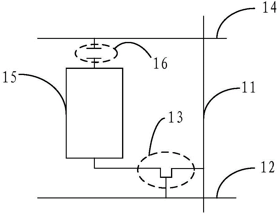
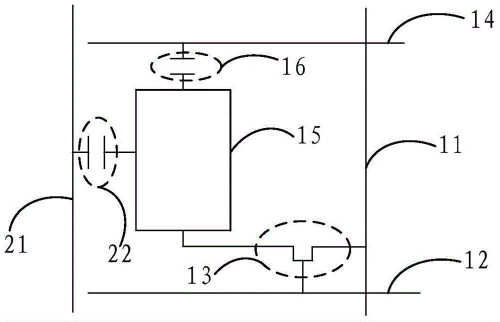
[0066] see image 3 A display panel provided by an embodiment of the present invention includes: a substrate (not shown in the figure), data lines 11 and gate lines 12 intersecting on the substrate, and sub-pixel units surrounded by the data lines and gate lines, Each sub-pixel unit includes a TFT13, a pixel electrode 15, a first common electrode 14 and a second common electrode 21, and the second common electrode 21 is connected to an input terminal for providing an AC voltage of a first frequency; wherein, the second common electrode 21 and the projection of the pixel electrode 15 on the substrate have overlapping areas.

[0067] It should be noted that the first frequency is generally greater than or equal to 120 Hz, and is used to provide high frequency to the second common electrode. The projection of the second common electrode 21 and the pixel electrode 15 on the substrate has an overlapping area, and the overlapping area makes a capacitor 22 formed between the second ...

Embodiment 2

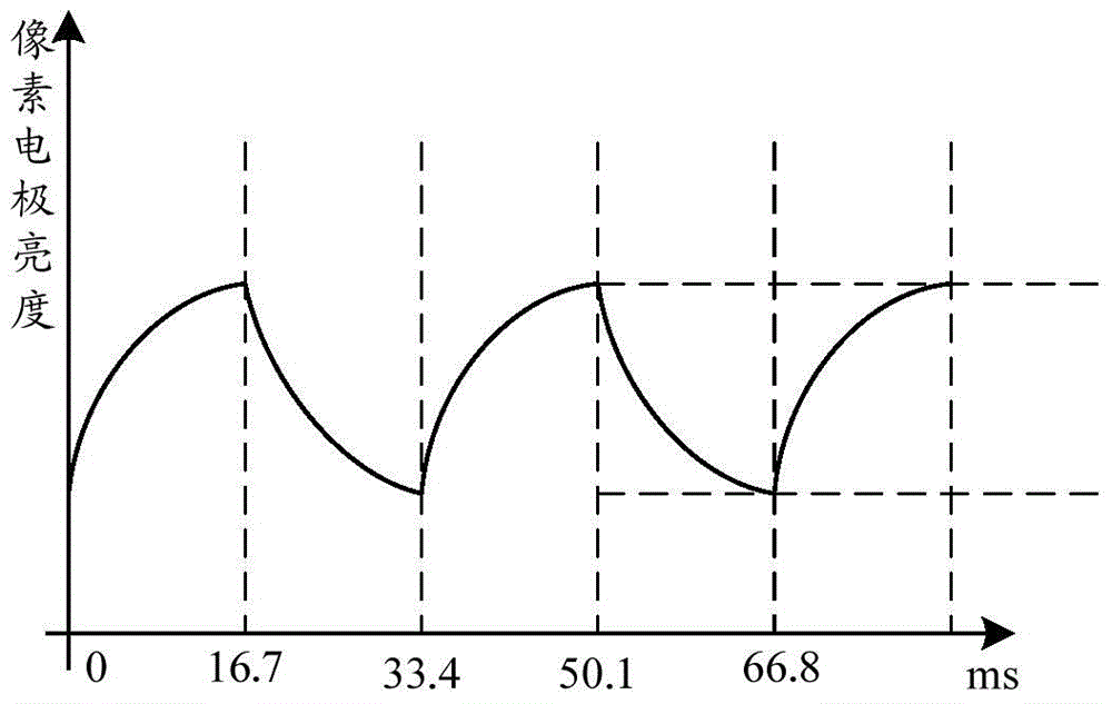
[0095] see Figure 4 , the embodiment of the present invention provides a method for using the display panel debugging screen flickering provided by the embodiment of the present invention, the method includes:

[0096] S401. Apply an AC voltage of the first frequency to the second common electrode;

[0097] It should be noted that the applied AC voltage of the first frequency is higher than the AC voltage of the second frequency provided by the data line.

[0098]S402. Determine the change value of the pixel electrode voltage in adjacent periods according to the change value of the AC voltage of the first frequency on the second common electrode;

[0099] It should be noted that, in the embodiment of the present invention, the change value of the AC voltage at the first frequency is defined as: the voltage difference before and after the change of the AC voltage. The variation value of the pixel electrode voltage in adjacent periods is: the voltage difference before and aft...


PUM


Abstract

The invention provides a display panel, a method and a device for debugging a flicker, and a display device; the method and the device for debugging the flicker are used for improving the flicker phenomenon in the display panel under the condition that the frequency of a pixel electrode to drive a liquid crystal to turn over is unchanged so that the flicker is not perceived easily by human eyes; the display panel comprises a substrate, data lines and grid lines arranged on the substrate crossly, and sub-pixel units enclosed by the data lines and the grid lines; the display panel is characterized in that each of the sub-pixel units comprises a TFT (thin film transistor), a pixel electrode, a first common electrode and a second common electrode, and the second common electrodes are connected with the input end used for providing an alternating current voltage of a first frequency, wherein projections, on the substrate, of the second common electrodes and the pixel electrodes have an overlapping area.

Description

technical field [0001] The invention relates to the field of liquid crystal displays, in particular to a display panel, a method and a device for flickering a debugging screen, and a display device. Background technique [0002] With the rapid development of digital technology, digital displays are constantly being updated. The display picture effect of the liquid crystal display panel is also constantly pursued by people. In the prior art, Thin Firm Transistor Liquid Crystal Display (TFT-LCD) has gradually become the current leading product because of its small size, low power consumption, no radiation, high resolution and other advantages. [0003] Generally, in practical applications, when the TFT-LCD screen is displayed, there will be a screen flicker (Flicker) problem. Generally, the characteristic of liquid crystal molecules is that they will always maintain a flip direction when the applied voltage remains unchanged. If the liquid crystal molecules stay in the same ...

Claims


Application Information

Patent Timeline
Patent Type & Authority Applications(China)
IPC IPC(8): G02F1/1343G02F1/133G09G3/36
CPCG02F1/13306G02F1/134309G09G3/006G09G3/3655G09G2230/00G09G2300/043G09G2320/0233G09G2320/0247G01R31/2825G02F1/133514G02F1/136286G02F1/1368G02F2201/123G02F1/134318
Inventor 严允晟
Owner BOE TECH GRP CO LTD
Why Eureka
Try Eureka