Shift register, gate drive circuit and liquid crystal display panel
A shift register and gate technology, applied in static memory, digital memory information, instruments, etc., can solve the problem of affecting the output capability of the gate drive circuit of the shift register, the large layout area of the voltage stabilizing capacitor, and the disadvantage of meeting the narrow frame of the user In order to achieve the effect of reducing the layout area, satisfying the narrow border, and improving the output capacity
- Summary
- Abstract
- Description
- Claims
- Application Information
AI Technical Summary
Problems solved by technology
Method used
Image

Examples
Embodiment 1
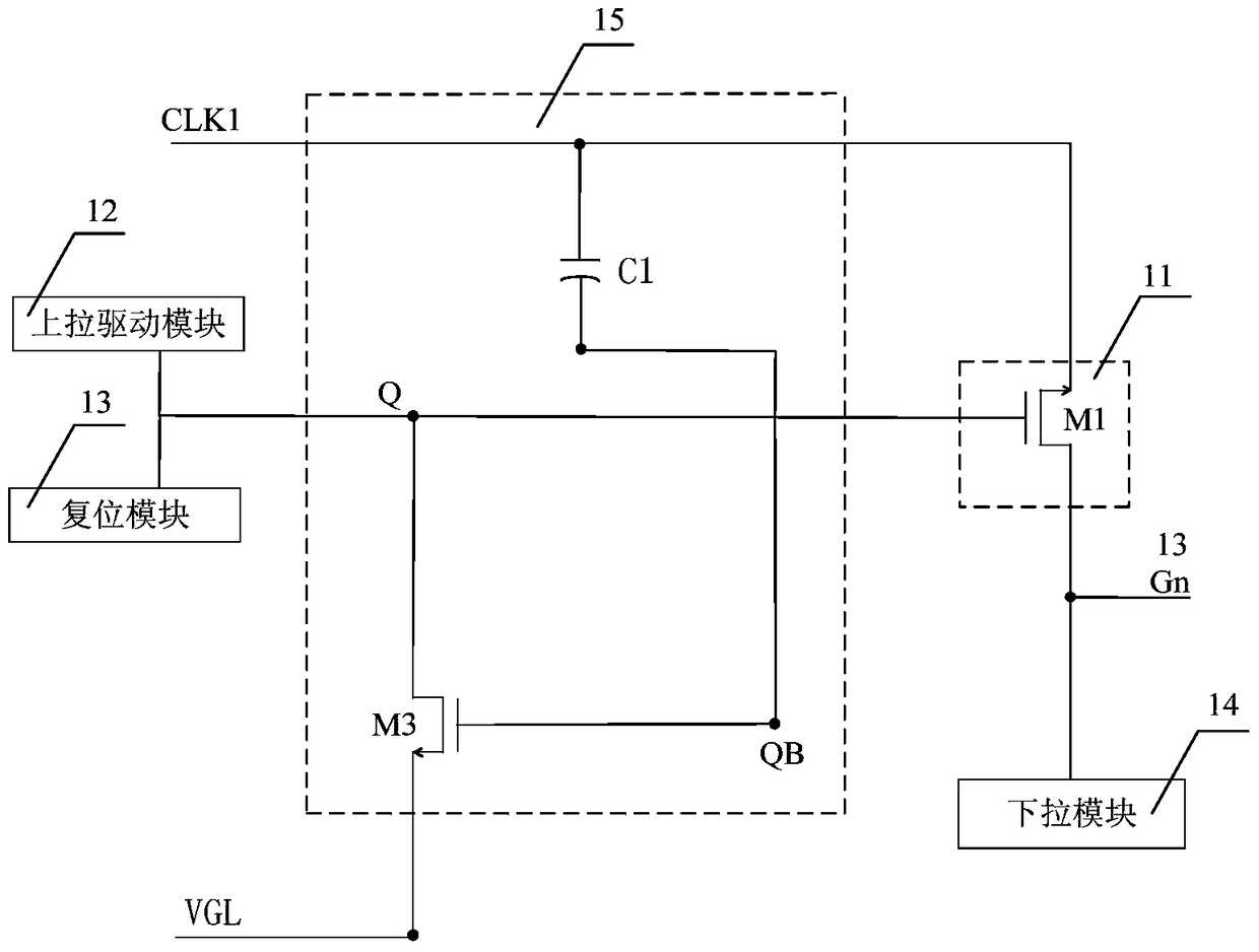
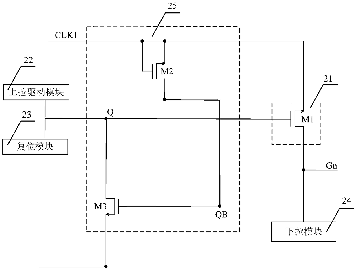
[0039]An embodiment of the present invention provides a shift register, figure 2 For the circuit structure diagram of the shift register provided in Embodiment 1 of the present invention, see figure 2 , the shift register includes a pull-up module 21, a pull-up drive module 22, a reset module 23, a pull-down module 24 and a voltage stabilizing module 25;
[0040] The pull-up module 21 includes a pull-up transistor M1, the source of the pull-up transistor M1 is electrically connected to the first clock signal line CLK1, the drain of the pull-up transistor M1 is electrically connected to the signal output end of the shift register, and the pull-up transistor M1 The gate of is electrically connected to the pull-up control node Q;
[0041] The output terminal of the pull-up driving module 22 is electrically connected to the pull-up control node Q, and is used to control the pull-up transistor M1 to turn on and output the scan signal;
[0042] The output terminal of the reset m...
Embodiment 2
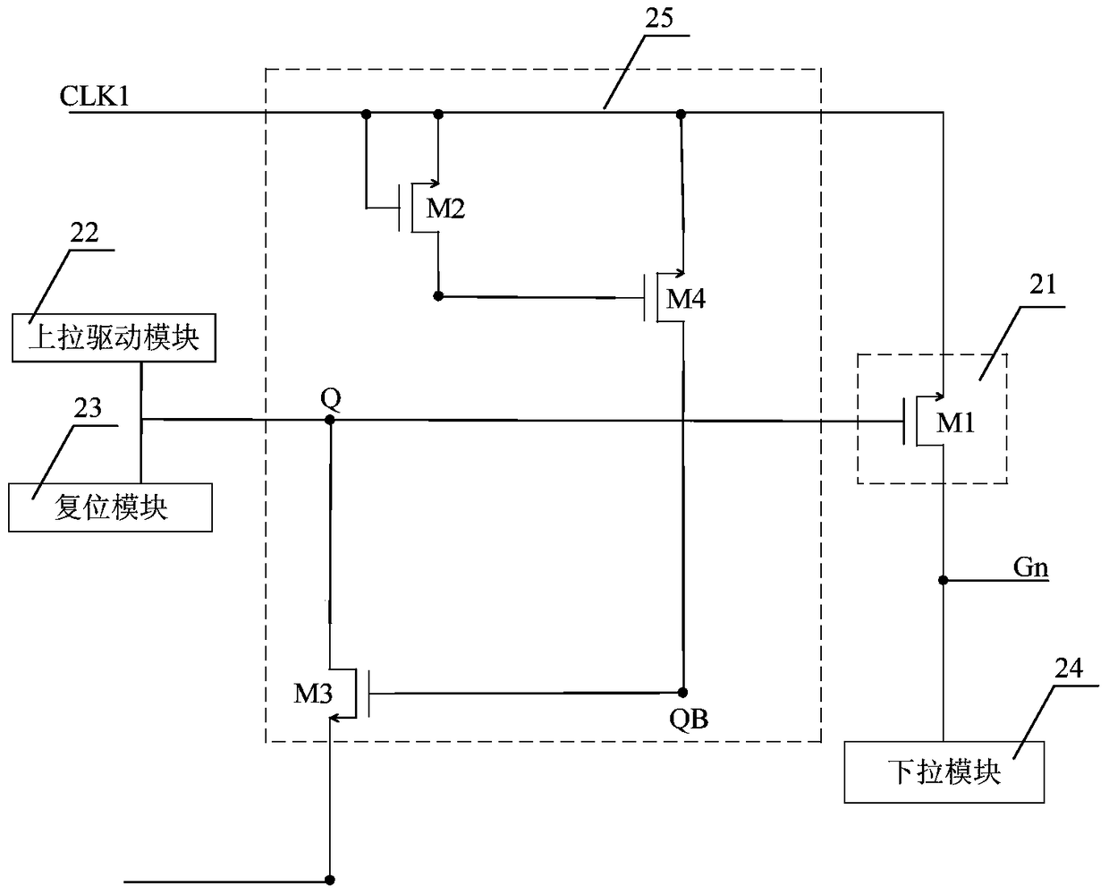
[0047] image 3 The circuit structure of the shift register provided for the second embodiment of the present invention Figure 1 ,Such as image 3 As shown, on the basis of Embodiment 1, the voltage stabilizing module of the shift register further includes a third voltage stabilizing transistor M4, the gate of the third voltage stabilizing transistor M4 is electrically connected to the drain of the first voltage stabilizing transistor M2, The source of the third voltage stabilizing transistor M4 is electrically connected to the first clock signal line CLK1 , and the drain of the third voltage stabilizing transistor M4 is electrically connected to the voltage stabilizing control node QB. The third voltage stabilizing transistor cooperates with the first voltage stabilizing transistor to control the potential on the voltage stabilizing control node QB to be consistent with the signal of the first clock signal line in the stable output stage.
[0048] further, Figure 4 The c...
Embodiment 3
[0051] In the third embodiment, the specific circuits of the pull-up driving module, the pull-down module and the reset module involved in the above-mentioned embodiments will be described.
[0052] Figure 5 The circuit structure diagram of the shift register provided for the third embodiment of the present invention, such as Figure 5 As shown, the pull-up drive module 22 includes a pull-up drive transistor M7, the gate of the pull-up drive transistor M7 is electrically connected to the signal output terminals of the first two stages of shift registers, and the input scan signal Gn-2 is used as the shift register of this stage. The trigger signal of the register, and the source of the pull-up driving transistor M7 is electrically connected to the second clock signal line CLK2, and the drain of the pull-up driving transistor M7 is electrically connected to the pull-up control node Q;
[0053] The reset module 23 includes a reset transistor M8, the gate of the reset transisto...
PUM
 Abstract
Description
Claims
Application Information
 - R&D
- Intellectual Property
- Life Sciences
- Materials
- Tech Scout
- Unparalleled Data Quality
- Higher Quality Content
- 60% Fewer Hallucinations
Browse by: Latest US Patents, China's latest patents, Technical Efficacy Thesaurus, Application Domain, Technology Topic, Popular Technical Reports.
© 2025 PatSnap. All rights reserved.Legal|Privacy policy|Modern Slavery Act Transparency Statement|Sitemap|About US| Contact US: help@patsnap.com