A synchronous clock system for multiple high-speed signals of a super-large area array cmos camera

A technology of synchronous clock and high-speed signal, applied in the direction of automatic power control, electrical components, etc., can solve the problem of unable to reduce jitter, unable to control the duty cycle, etc., to solve the design layout and wiring, difficult to change the duty cycle, reduce The effect of small transmission distance

Active Publication Date: 2017-07-28
BEIJING RES INST OF SPATIAL MECHANICAL & ELECTRICAL TECH
View PDF5 Cites 0 Cited by
  • Summary
  • Abstract
  • Description
  • Claims
  • Application Information

AI Technical Summary

Problems solved by technology

Patent CN102882623A proposes a configurable clock frequency synthesis device based on FPGA, which can generate clock signals of various frequencies, but because the generated clock signals are all homologous, the duty cycle and jitter of the signals are different It mainly depends on the clock quality provided by the crystal oscillator to the FPGA, so it cannot reduce the jitter, nor can it control the duty cycle

Method used


Image

  • A synchronous clock system for multiple high-speed signals of a super-large area array cmos camera
  • A synchronous clock system for multiple high-speed signals of a super-large area array cmos camera
  • A synchronous clock system for multiple high-speed signals of a super-large area array cmos camera

Examples


Embodiment Construction

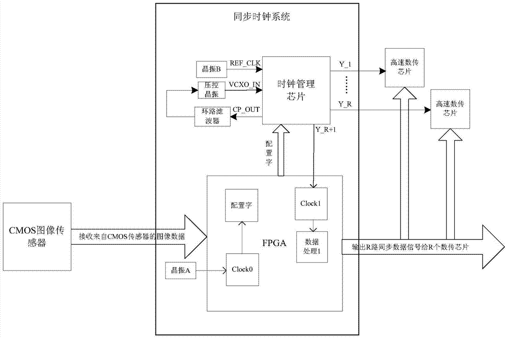
[0025] According to the characteristics of super large area array CMOS camera image transmission, and output multiple high-speed signals at the same time, the present invention designs a working crystal oscillator A, a reference crystal oscillator B, T voltage-controlled crystal oscillators, a programmable logic device FPGA, and T phase-locked loops Functional clock management chip, T loop filter clock system, the specific structure is as follows figure 1 shown. The system uses T clock management chips, voltage-controlled crystal oscillators, loop filters, and a reference crystal oscillator B to form T phase-locked loop structures, which can simultaneously output T*R synchronous clocks with the same phase, where T≥ 2. R≥2, T and R are both positive integers, and R is the number of synchronous clock channels that each clock management chip can output to subsequent R high-speed data transmission chips.

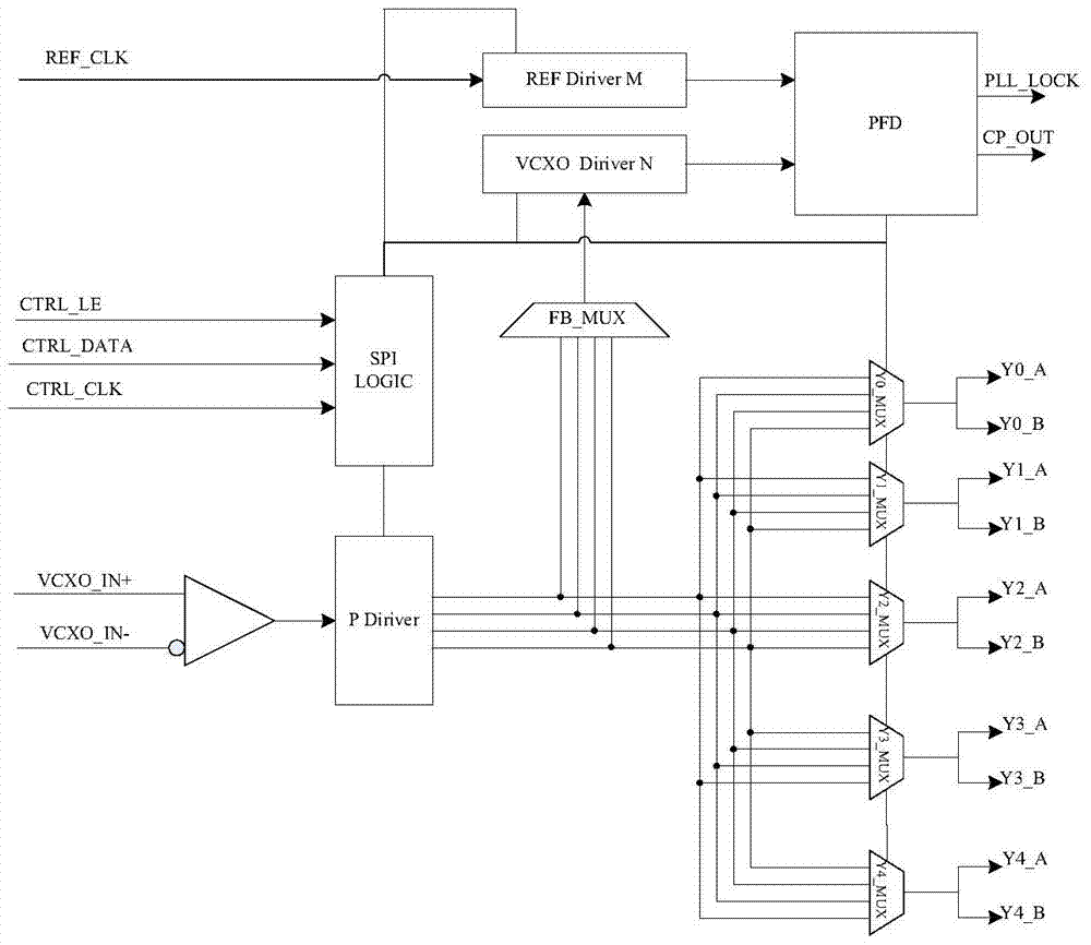
[0026] The clock management chip generally needs to be configured by the F...


PUM


Abstract

The invention discloses a synchronized clock system for ultra-large area array CMOS camera multipath high-speed signals. The system comprises a work crystal oscillator, a reference crystal oscillator, T voltage controlled crystal oscillators, a programmable logic device (FPGA), T clock management chips having phase-locked loop functions, and T loop filters, wherein T is a positive integer. A phase-locked loop is formed by one clock management chip, the reference crystal oscillator, one voltage controlled crystal oscillator and one loop filter. Each phase-locked loop performs frequency division on the output frequency of the corresponding voltage controlled crystal oscillator according to input frequency division control quantities, and generates R+1 paths of data synchronized clocks. According to the invention, the system employs one reference crystal oscillator to output homologous reference frequency, so that T*R paths of synchronized clocks having consistent phases can be output, and a clock synchronization problem of multipath signals is solved. Furthermore, the clock management chips are employed to provide work clocks for the FPGA, and image data is processed by the corresponding clocks, so that the synchronization of output clocks and data phases of the FPGA can be completely guaranteed.

Description

technical field [0001] The invention relates to a signal synchronous clock system, which is especially suitable for image data transmission of a large area array CMOS image sensor camera system of space remote sensing satellites. Background technique [0002] With the increasing demand of remote sensing users for high-resolution continuous reconnaissance and surveillance, the application advantages of large area array CMOS sensors in high-orbit remote sensing satellites have gradually become prominent. Since the large area array CMOS sensor can output multiple high-speed image signals at the same time, it puts forward higher requirements for data transmission. Simultaneous transmission of multiple high-speed signals requires the use of multiple high-speed digital transmission chips, but too many chips will make the layout of the chip uncompact, which inevitably leads to long-distance transmission problems, which will make the ordinary clock transmitted by the FPGA Duty cycl...

Claims


Application Information

Patent Timeline
Patent Type & Authority Patents(China)
IPC IPC(8): H03L7/08H03L7/18
Inventor 郭宇琨王衍王建宇于双江荣鹏程甘霖王鑫张旭
Owner BEIJING RES INST OF SPATIAL MECHANICAL & ELECTRICAL TECH
Why Eureka
Try Eureka