Display panel, manufacturing method thereof and display device

A technology for display panels and display areas, applied in lamination devices, chemical instruments and methods, transportation and packaging, etc., can solve problems such as easy breakage, light leakage, Mura, etc., to improve strength and reliability, increase thickness, avoid The effect of black screen

Inactive Publication Date: 2015-08-19
BOE TECH GRP CO LTD +1
View PDF10 Cites 11 Cited by
  • Summary
  • Abstract
  • Description
  • Claims
  • Application Information

AI Technical Summary

Problems solved by technology

The stress is transmitted to the visible area of ​​the display panel, causing defects such as light leakage and mura
The entire COG process and adverse phenomena
In addition, for the display device based on the above-mentioned display panel (a backlight is also provided on the basis of the display panel), since the driver IC and FPC need to be bound to the top of the array substrate, since the thickness of this part is usually relatively thin, only other parts of the overall display panel Half of the thickness, in addition to the poor Mura caused by the COG process, this area is also prone to damage during the drop test

Method used


Image

  • Display panel, manufacturing method thereof and display device
  • Display panel, manufacturing method thereof and display device
  • Display panel, manufacturing method thereof and display device

Examples


Embodiment 1

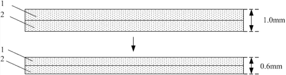
[0039] This embodiment provides a method for preparing a display panel and a display panel formed by using the method. By using the method, a partially thinned display panel can be easily formed, so that display panels with different thicknesses can be formed in partitions, and can simultaneously adapt to The driver IC is attached and the strength of the display panel is ensured to better realize the thinning of the display panel; and the thickness of the display area of ​​the display panel is ensured to avoid light leakage and COG Mura defects.

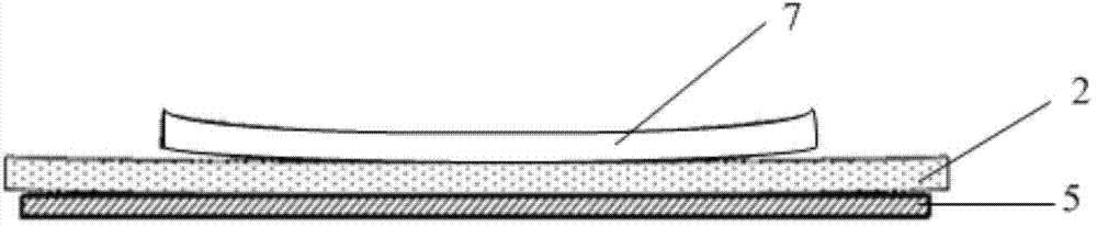
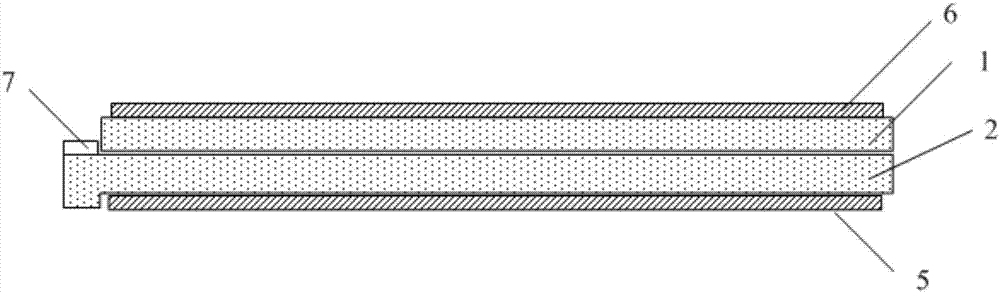
[0040] This embodiment provides a display panel, the two sides of the display panel are respectively the first surface and the second surface, such as figure 2 As shown, the display panel includes a first substrate and a second substrate opposite to each other (the outer side of the first substrate relative to the second substrate is the first surface, and the outer side of the second substrate relative to the first substrate is the ...

Embodiment 2

[0087] This embodiment provides a display device, including the display panel in Embodiment 1.

[0088] On the substrate of the display panel in Embodiment 1, taking the liquid crystal display panel as an example, the backlight source 10 is assembled according to the normal assembly process, that is, the following Figure 5 The display device shown.

[0089] The display device can be any product or component with a display function such as a liquid crystal panel, an electronic paper, an OLED panel, a mobile phone, a tablet computer, a television, a monitor, a notebook computer, a digital photo frame, a navigator, and the like.

[0090] The display device adopts the above-mentioned display panel, so it has better display effect.


PUM


Abstract

The invention belongs to the technical field of display, and particularly relates to a display panel, a manufacturing method thereof and a display device. The display panel comprises a first substrate and is divided into a display area and a non-display area, and the non-display area of the first substrate comprises an IC attaching area. The manufacturing method includes the step of thinning. The manufacturing method is characterized in that the step of thinning includes: 1), forming a barrier layer insoluble in thinning liquid in an area, corresponding to the IC attaching area, of the first surface of the first substrate of the display panel; 2), adopting the thinning liquid to thin the display panel to enable thickness of the IC attaching area of the first substrate to be larger than that of the display area; 3), removing the barrier layer. Zones, different in thickness, of the display panel are formed through local thinning, suitability of attaching of a driving IC is realized while strength of the display panel is guaranteed, and thinning of the display panel is realized; thickness of the display area of the display panel is guaranteed, so that light leakage and bad COG Mura effect are avoided.

Description

technical field [0001] The invention belongs to the field of display technology, and in particular relates to a method for preparing a display panel, a display panel, and a display device. Background technique [0002] The liquid crystal display panel includes a display panel cell, a printed circuit board PCB, a driver IC, etc., where the cell and the driver IC are generally connected by means of COG (Chip On Glass) through ACF (Anisotropic Conductive Adhesive), and the PCB and the cell are connected through a flexible circuit board. FPC connection. [0003] Now, small-sized liquid crystal display panels are more and more inclined to be ultra-thin and ultra-high-resolution in the market. Along with users' requirements for product quality, designers' demands for panel edge area, and manufacturers' cost control, driving The IC is developing towards multi-pin and narrow and long, and the length of the driving IC is increased to meet the resolution requirements; while the liqui...

Claims


Application Information

Patent Timeline
Patent Type & Authority Applications(China)
IPC IPC(8): G02F1/1333
CPCG02F1/1333G02F1/133302G02F1/133351H01L27/1262B32B7/04B32B3/263B32B2250/04B32B2255/26B32B2307/40B32B2307/50B32B2307/732B32B2457/202B32B2457/206B32B7/05B32B37/18B32B38/10B32B2307/202B32B2307/42B32B2310/0409B32B2457/20H01L27/1259G02F1/133368G02F1/133388H10K50/84H10K59/38H10K59/1213H10K71/00B32B3/30B32B2309/02G02F1/133514G02F1/133528G02F1/1341H01L25/0657H01L25/50H01L27/124
Inventor 杨刚龙君
Owner BOE TECH GRP CO LTD
Why Eureka
Try Eureka