Method for improving electroplating layer uniformity of PCB (printed circuit board) vertical electroplating line

A vertical electroplating and electroplating layer technology, applied in the direction of electrodes, electrolytic process, electrolytic components, etc., to achieve the effects of uniform power lines, reduced copper consumption, and uniform current distribution

Inactive Publication Date: 2015-09-02
SHENZHEN SUNTAK MULTILAYER PCB
View PDF5 Cites 14 Cited by
  • Summary
  • Abstract
  • Description
  • Claims
  • Application Information

AI Technical Summary

Problems solved by technology

[0004] For this reason, the technical problem to be solved by the present invention is to solve the problem of eliminating the current distribution potential difference between the cathode and the anode when they have different length differences.

Method used


Image

  • Method for improving electroplating layer uniformity of PCB (printed circuit board) vertical electroplating line

Examples


Embodiment 1

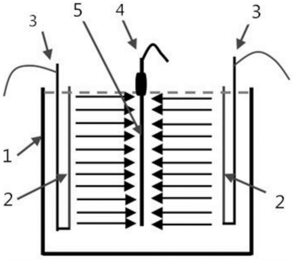
[0027] combined with figure 1 As shown, the present embodiment discloses a method for improving the uniformity of the electroplating layer of PCB vertical electroplating lines, including the following steps:

[0028] S1: The lower ends of the two anodes 2 in the electroplating copper cylinder 1 are respectively connected to the corresponding conductive rods 3;

[0029] S2: Connect the two conductive rods to the anode 2 of the rectifier;

[0030] S3: connecting the flying target 4 in the electroplating copper cylinder to the cathode of the rectifier;

[0031] S4: hang the PCB production board 5 on the flying target;

[0032] S5: setting the anode 2 current introduction point at the lower end of the conductive rod;

[0033] S6: energize the cathode and anode, and perform electroplating treatment on the PCB production board 5 to be electroplated.

[0034] Wherein, the upper end of the PCB production board 5 is clamped on the flying target; and the electroplating current is se...


PUM


Abstract

The invention belongs to the field of circuit board processing, and relates to a method for improving the electroplating uniformity of a PCB (printed circuit board). By adopting the method disclosed by the invention, an anode is converted into an up-and-down sliding mode from a position fixing mode so as to ensure that the vertical length difference between a cathode and the anode can be eliminated, and uniform current distribution in an electroplating process can be ensured; a conventional wire connection mode of the anode can be changed so as to ensure that the electrical potential size difference of the current distribution of the anode can be changed and can be complementary with the electrical potential size difference of the current distribution of the cathode; the uniformity of an electroplating copper layer can be improved, and the copper consumption per unit area can be reduced; in a copper electroplating process, integral resistance in an electroplating cylinder is relatively balanced, so that power lines distributed in the electroplating cylinder are uniform, and thus the electrical potential size difference of upper and lower current distribution in the electroplating cylinder can be effectively eliminated; and by adopting the electroplating copper layer with good uniformity, difficulties of circuit etching can be reduced, the purposes of reducing the production scrap rate and improving the quality of the PCB can be achieved, and great market economic values and application prospects can be achieved.

Description

technical field [0001] The invention belongs to the field of circuit board processing, in particular to a method for improving the uniformity of the electroplating layer of a PCB vertical electroplating line. Background technique [0002] At present, there are two types of PCB electroplating copper technology: soluble anode and insoluble anode. The soluble anode uses titanium blue copper ball as the anode directly, and the insoluble anode uses stainless steel or titanium mesh as the anode. Both methods are passed in the electroplating cylinder. Install anode baffles and cathode floating racks to block high-potential currents so that the overall current distribution is relatively uniform. [0003] In the prior art, soluble anodes have uneven anode area distribution, resulting in relatively poor uniformity of the electroplated copper layer, while insoluble anodes have uniform anode area distribution, and the uniformity of the electroplated copper layer is relatively good. The...

Claims


Application Information

Patent Timeline
Patent Type & Authority Applications(China)
IPC IPC(8): C25D7/00C25D17/00C25D17/10
Inventor 常文智彭卫红刘东韩焱林
Owner SHENZHEN SUNTAK MULTILAYER PCB
Why Eureka
Try Eureka