Electroluminescent device and fabrication method thereof

a technology of electroluminescent devices and fabrication methods, which is applied in the testing/measurement of individual semiconductor devices, semiconductor/solid-state devices, instruments, etc., can solve the problems of increasing the complexity of production processes, and reducing the yield of led devices, so as to reduce the cost of production. , the effect of preventing current clogging

Active Publication Date: 2008-06-19
XIAMEN SANAN OPTOELECTRONICS CO LTD
View PDF3 Cites 10 Cited by
  • Summary
  • Abstract
  • Description
  • Claims
  • Application Information

AI Technical Summary

Benefits of technology

[0010]The present invention provides an electroluminescent device and a fabrication method thereof that involve simple production processes, possess a uniform electrical current distribution, and are capable of reducing heat accumulation.
[0014]As mentioned above, an electroluminescent device and a fabrication method thereof according to the present invention utilize a conduction substrate that connects the contact electrodes of the LED element disposed at opposite sides of the conduction substrate. In comparison with the prior art, because the etching process is avoided, the production processes are thus simplified and the yield is raised. In addition, the patterned transparent conduction layer with a plurality of island-like structures is formed by for example the etching method so that the electrical current imposed to the LED element can be uniformly distributed so as to prevent current clogging. Moreover, the deposition of the reflection layer has a good ohmic contact with the patterned transparent conduction layer and provides a scattering and reflection interface. It effectively raises external light extraction and light emitting efficiency. Also, since the conduction substrate and the reflection layer are highly thermally conductive, the heat generated from the LED element can be more effectively dissipated than the prior art.

Problems solved by technology

However, in addition to increase the complexity of the production process, this step may cause a leakage current of the LED element 10 due to its uneven surface as a result of the bad control in etching.
This will lower the yield of the LED device 1.
Since the epitaxial substrate and the organic adhering material have low thermal conductivity coefficients, they cannot provide a better heat dissipation path for the LED element 10.
As a result, the heat generated from the operating LED device 1 accumulates and affects the light emitting efficiency thereof.

Method used


Image

  • Electroluminescent device and fabrication method thereof
  • Electroluminescent device and fabrication method thereof
  • Electroluminescent device and fabrication method thereof

Examples


Embodiment Construction

[0020]The present invention will be apparent from the following detailed description, which proceeds with reference to the accompanying drawings, wherein the same references relate to the same elements.

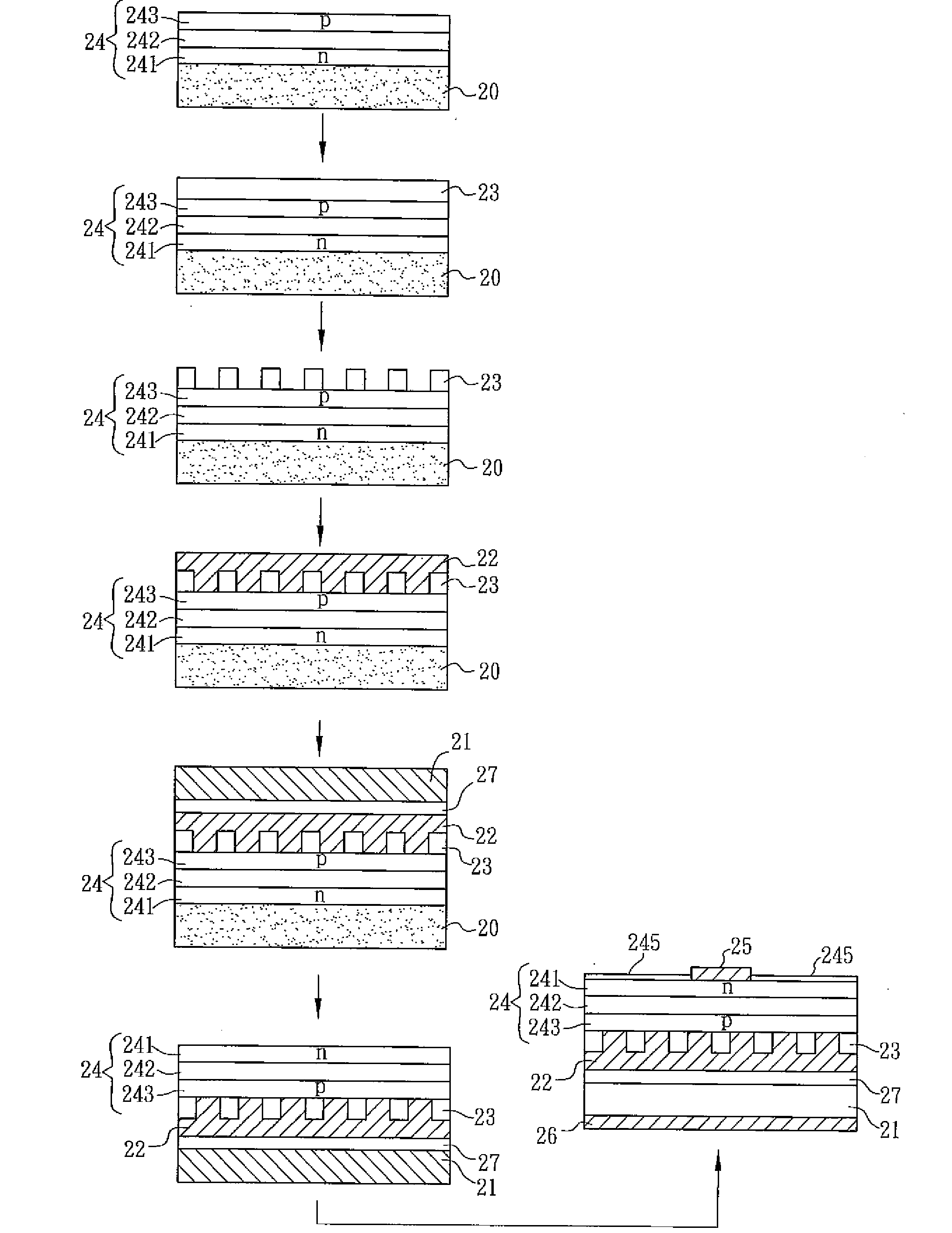
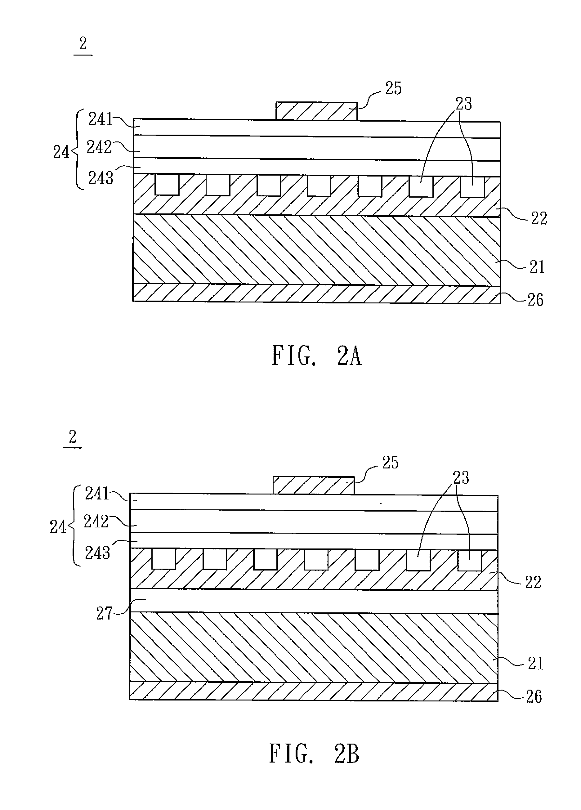
[0021]Please refer to FIGS. 2A, 2B, 3A and 3B. An electroluminescent device 2 according to a preferred embodiment of the present invention includes a conduction substrate 21, a reflection layer 22, a patterned transparent conduction layer 23, at least one light emitting diode (LED) element 24, a first contact electrode 25 and a second contact electrode 26.

[0022]In this embodiment the conduction substrate 21 can be made of a semiconductor material or a metal that having a high coefficient of thermal conductivity. The semiconductor material is selected from the group consisting of Si, GaAs, GaP, SiC, BN and their combinations. The metal is selected from the group consisting of Al, Cu, Ag, Au, Ni and their combinations.

[0023]The reflection layer 22 is formed on the conduction substrate 2...


PUM


Abstract

An electroluminescent device includes a conduction substrate, a reflection layer, a patterned transparent conduction layer, at least one light emitting diode (LED) element, a first contact electrode and a second contact electrode. The reflection layer is disposed on the conduction substrate, and the patterned transparent conduction layer is formed on the reflection layer. The LED element is formed on the patterned transparent conduction layer, and the LED element includes a first semiconductor layer, a light emitting layer and a second semiconductor layer in sequence. The second semiconductor layer is disposed on the patterned transparent conduction layer and the reflection layer. The first contact electrode is disposed at one side of the first semiconductor layer, and the second contact electrode is disposed at one side of the conduction substrate.

Description

CROSS REFERENCE TO RELATED APPLICATIONS[0001]This Non-provisional application claims priority under 35 U.S.C. §119(a) on Patent Application No. 09,514,7369, filed in Taiwan, Republic of China on Dec. 18, 2006, the entire contents of which are hereby incorporated by reference.BACKGROUND OF THE PRESENT INVENTION[0002]1. Field of Invention[0003]The present invention relates to an electroluminescent device and a fabrication method thereof, and more particularly to an electroluminescent device and a fabrication method thereof with high efficiency.[0004]2. Related Art[0005]The light emitting diode (LED) is a cold light emitting element, which releases lights when energy released after electrons and holes are combined in a semiconductor material. According to different used materials, various monochromatic lights with different wavelengths are outputted. The LEDs may be mainly classified into a visible light LED and an invisible light (infrared) LED. Compared with the conventional lighting...

Claims


Application Information

Patent Timeline
Patent Type & Authority Applications(United States)
IPC IPC(8): H01L33/00H01L33/38H01L33/40H01L33/42
CPCH01L33/0079H01L33/387H01L2933/0091H01L33/42H01L33/405H01L33/0093
Inventor CHEN, SHIH-PENGSHIUE, CHING-CHUANLIAO, HSUEH-KUOCHENG, CHUAN-CHIACHEN, HUANG-KUN
Owner XIAMEN SANAN OPTOELECTRONICS CO LTD
Why Eureka
Try Eureka