Light modulation element

一种光调制元件、相位调制的技术,应用在光学元件、光学、光导等方向,能够解决调制效率降低、调制带域降低、电信号传播损失大等问题,达到抑制传播损失、缩短距离的效果

Inactive Publication Date: 2015-09-02
FUJIKURA LTD
View PDF6 Cites 16 Cited by
  • Summary
  • Abstract
  • Description
  • Claims
  • Application Information

AI Technical Summary

Problems solved by technology

However, it is known that the propagation loss of electrical signals in the traveling-wave electrode on the silicon substrate is large, and if the electrodes other than the phase modulator 124 are longer, the modulation efficiency will be reduced due to the power loss of the electrical signal, resulting in a high The frequency loss becomes more prominent and the modulation band is lowered

Method used


Image

  • Light modulation element
  • Light modulation element
  • Light modulation element

Examples


no. 1 Embodiment approach

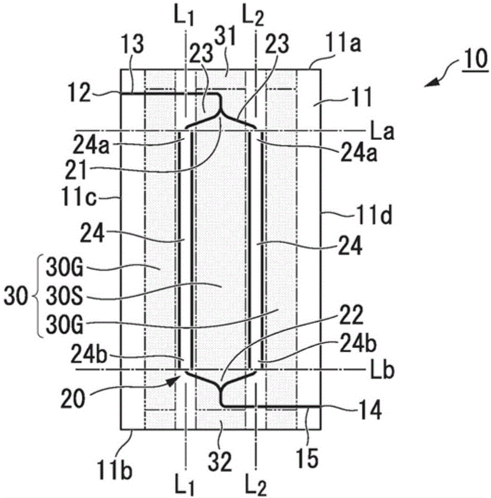
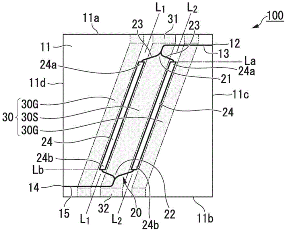
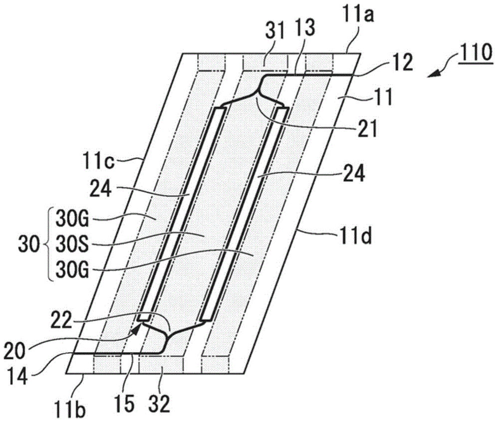
[0130] Figure 1A ~ Figure 1C The light modulation element according to the first embodiment of the present invention is shown. The optical modulation elements 10 , 100 , and 110 are constituted by a substrate-type optical waveguide 11 including a Mach-Zehnder interferometer 20 . The Mach-Zehnder interferometer 20 has two arm parts between a 1×2 optical branching unit (first optical branching unit) 21 and a 2×1 optical multiplexing unit (first optical multiplexing unit) 22 twenty three. The light incident on the light branching part 21 from the light incident part 12 via the optical waveguide 13 is branched into two arm parts 23 by the light branching part 21 . Thereafter, the branched light is multiplexed into one light by the optical multiplexing unit 22 through the two arm portions 23 , and the multiplexed light is emitted from the light emitting unit 14 through the optical waveguide 15 .

[0131] also, Figure 1B as well as Figure 1C The light modulating elements 100...

no. 2 Embodiment approach

[0155] Figure 3A and 3B represent the light modulation element according to the second embodiment of the present invention. In addition, in the following description, the same code|symbol is attached|subjected to the structure common to what was already demonstrated, and overlapping description is abbreviate|omitted.

[0156] The light modulation elements 10A and 100A according to the present embodiment are constituted by the substrate-type optical waveguide 11 including the Mach-Zehnder interferometer 20 similarly to the light modulation elements 10 , 100 , and 110 of the first embodiment. In addition, in the present embodiment, the light incident part 12 and the light emitting part 14 are located on two sides extending from the two end parts 24a, 24b in the longitudinal direction of the phase modulation part 24 in directions parallel to the two sides 11a, 11b, respectively. The area between the lines La and Lb.

[0157] Here, the traveling-wave electrode 30 is defined as ...

no. 3 Embodiment approach

[0168] Figure 4A as well as Figure 4B A light modulation element according to a third embodiment of the present invention is shown. The light modulation elements 10B and 100B according to the present embodiment are constituted by the substrate-type optical waveguide 11 including the Mach-Zehnder interferometer 20 similarly to the light modulation elements 10 and 100 of the first embodiment. In addition, in Figure 4A In the optical modulation element 10B, the long-side direction of the phase modulator 24 is perpendicular to the two sides 11a, 11b. On the other hand, in Figure 4B In the optical modulation element 100B, the longitudinal direction of the phase modulator 24 is inclined with respect to the two sides 11a and 11b.

[0169] In addition, in this embodiment, each arm unit 23 of the Mach-Zehnder interferometer 20 has an electrically independent phase adjustment unit (second phase adjustment unit) 25 different from the phase modulation unit (first phase adjustment u...


PUM

PropertyMeasurementUnit
refractive indexaaaaaaaaaa
impedanceaaaaaaaaaa
refractive indexaaaaaaaaaa

Abstract

A light modulation element configured from a substrate-type optical waveguide is provided with: a light incidence part through which light is incident on the substrate-type optical waveguide; a Mach-Zehnder interferometer comprising a first light branching part which branches the light incident on the light incidence part, two arm parts which guide the light branched by the first light branching part, a phase modulation part which is linearly provided in at least one of the two arm parts, and a first light multiplexing part which multiplexes the light guided from the two arm parts; a light emission part which emits the light multiplexed by the first light multiplexing part from the substrate-type optical waveguide; and a traveling wave electrode which has an input part and an output part and applies voltage to the phase modulation part. The substrate-type optical waveguide has an outline including two sides each crossing an extension line in the longitudinal direction of the phase modulation part in plan view, the input part is formed in one of the two sides, and the light incidence part and the light emission part are each located in a region different from a region in which the traveling wave electrode is formed in plan view.

Description

technical field [0001] The present invention relates to the construction of optical waveguide elements fabricated on substrates, and more particularly to the design of electrodes and optical waveguides for light modulating elements. This application claims priority based on Japanese Patent Application No. 2012-284723 filed in Japan on December 27, 2012, and Japanese Patent Application No. 2012-284724 filed in Japan on December 27, 2012, and uses the contents thereof here. Background technique [0002] Today, the amount of information utilized in optical communications is increasing. In order to cope with such an increase in the amount of information, in optical communication networks such as backbone networks, metropolitan networks, and access networks, countermeasures such as an increase in signal speed and an increase in the number of channels by wavelength multiplexing communication have been developed. Accompanying this countermeasure, problems have arisen such as the s...

Claims


Application Information

Patent Timeline
Patent Type & Authority Applications(China)
IPC IPC(8): G02F1/025G02B6/12G02B6/122
CPCG02F1/025G02B2006/12142G02B2006/12159G02F1/2255G02B6/122G02F2201/58G02B6/29353G02B6/29355G02B6/1228G02B6/125G02B2006/12097G02F1/212G02B2006/12147G02F1/218G02F1/2257
Inventor 五井一宏石原启树小川宪介小田研二日下裕幸松本亮吉植村仁
Owner FUJIKURA LTD
Why Eureka
Try Eureka