Full-digital debouncing circuit and method

A de-jitter, all-digital technology, applied in pulse shaping and other directions, can solve problems such as phase delay, square wave signal duty cycle change, etc., to reduce delay and ensure the effect of duty cycle

Inactive Publication Date: 2015-09-09
ZHEJIANG UNIV
View PDF3 Cites 21 Cited by
  • Summary
  • Abstract
  • Description
  • Claims
  • Application Information

AI Technical Summary

Problems solved by technology

[0007] Aiming at the problem that the duty cycle of the processed square wave signal changes relative to the original signal and there is a phase delay in the existing de-jittering method,

Method used


Image

  • Full-digital debouncing circuit and method
  • Full-digital debouncing circuit and method
  • Full-digital debouncing circuit and method

Examples


Embodiment Construction

[0027]The full digital debounce circuit and method of the present invention will be described in further detail below in conjunction with the accompanying drawings and specific implementation methods, but the examples are not intended to limit the present invention.

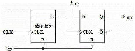
[0028] A realization circuit of an all-digital debounce method, comprising:

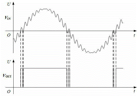
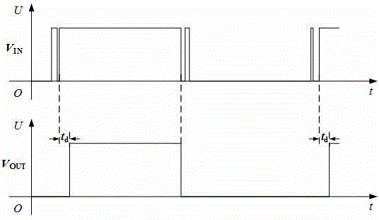
[0029] The edge detection circuit is used to receive the input square wave signal to be debounced, use the high-frequency clock to sample the input signal, and detect the rising edge and falling edge of the input signal;

[0030] Digital clipping circuit, which uses counting to delay the signal, that is, performs clipping processing;

[0031] The sampling circuit is used for signal sampling to obtain a clean and jitter-free square wave signal.

[0032] For the convenience of understanding the full digital debounce circuit of the present invention, Figure 4 A specific schematic diagram of the debounce circuit of the present invention ...


PUM


Abstract

The invention discloses a full-digital debouncing circuit and a full-digital debouncing method. The debouncing circuit comprises an edge detection circuit, a digital clipping circuit and a sampling circuit. The edge detection circuit is composed of two D triggers and an XNOR gate and is used for detecting a rising edge and a falling edge of an input square signal with jitter; the digital chipping circuit is composed of counter with an asynchronous reset end and the D trigger and is used for chipping the signal; the sampling circuit is composed of two D triggers and is used for sampling the signal so as to output clean square signal finally. Compared with the debouncing method such as current digital chipping, the debouncing method presented by the invention can be used for reducing delay of introducing the digital chipping while effectively debouncing to ensure duty ratio of the square signal. The full-digital debouncing circuit and the full-digital debouncing method of the invention are particularly applied to the application field that moving phase triggering control has relative strict phase requirement.

Description

technical field [0001] The invention relates to an integrated circuit technology, in particular to an all-digital debounce circuit capable of obtaining low-delay and reliable square waves. Background technique [0002] In any circuit design, the correctness of the signal is very important. When there is jitter in the signal, it often causes false triggering of the circuit, which leads to the operation error of the entire circuit system. Square wave signals are widely used in the field of integrated circuits. Due to noise and interference in the actual environment, there is jitter near the rising and falling edges of square wave signals entering the circuit, such as button signals, comparator outputs, etc., such as figure 1 The input signal shown is noisy. After passing through the zero-crossing comparator, there are relatively dense pulse jitters near the rising and falling edges of the output square wave. These pulse signals will cause the malfunction of the next-stage circ...

Claims


Application Information

Patent Timeline
IPC IPC(8): H03K5/08
Inventor 钱雨霁韩雁孙俊
Owner ZHEJIANG UNIV
Why Eureka
Try Eureka