Shell with two-dimensional circuit structure and manufacturing method thereof

A technology of circuit structure and manufacturing method, which is applied in the direction of cabinet/cabinet/drawer parts, input/output process of data processing, instruments, etc., can solve the problems of poor conductivity and high manufacturing cost, and reduce manufacturing cost. , easy to manufacture, the effect of mature process technology

Active Publication Date: 2018-06-29
TAIWAN GREEN POINT ENTERPRISE
View PDF8 Cites 0 Cited by
  • Summary
  • Abstract
  • Description
  • Claims
  • Application Information

AI Technical Summary

Problems solved by technology

[0005] Compared with the above-mentioned method of forming patterned circuit wires on an insulating substrate, the above-mentioned Taiwan Patent No. I360073 needs to use a flexible circuit board, which has high manufacturing costs, and uses indium tin oxide (ITO) as a flexible circuit board as a conductive material The conductivity is worse than that of patterned circuit wires formed directly on an insulating substrate

Method used


Image

  • Shell with two-dimensional circuit structure and manufacturing method thereof
  • Shell with two-dimensional circuit structure and manufacturing method thereof
  • Shell with two-dimensional circuit structure and manufacturing method thereof

Examples


Embodiment Construction

[0041] The present invention will be described in detail below in conjunction with the accompanying drawings and embodiments.

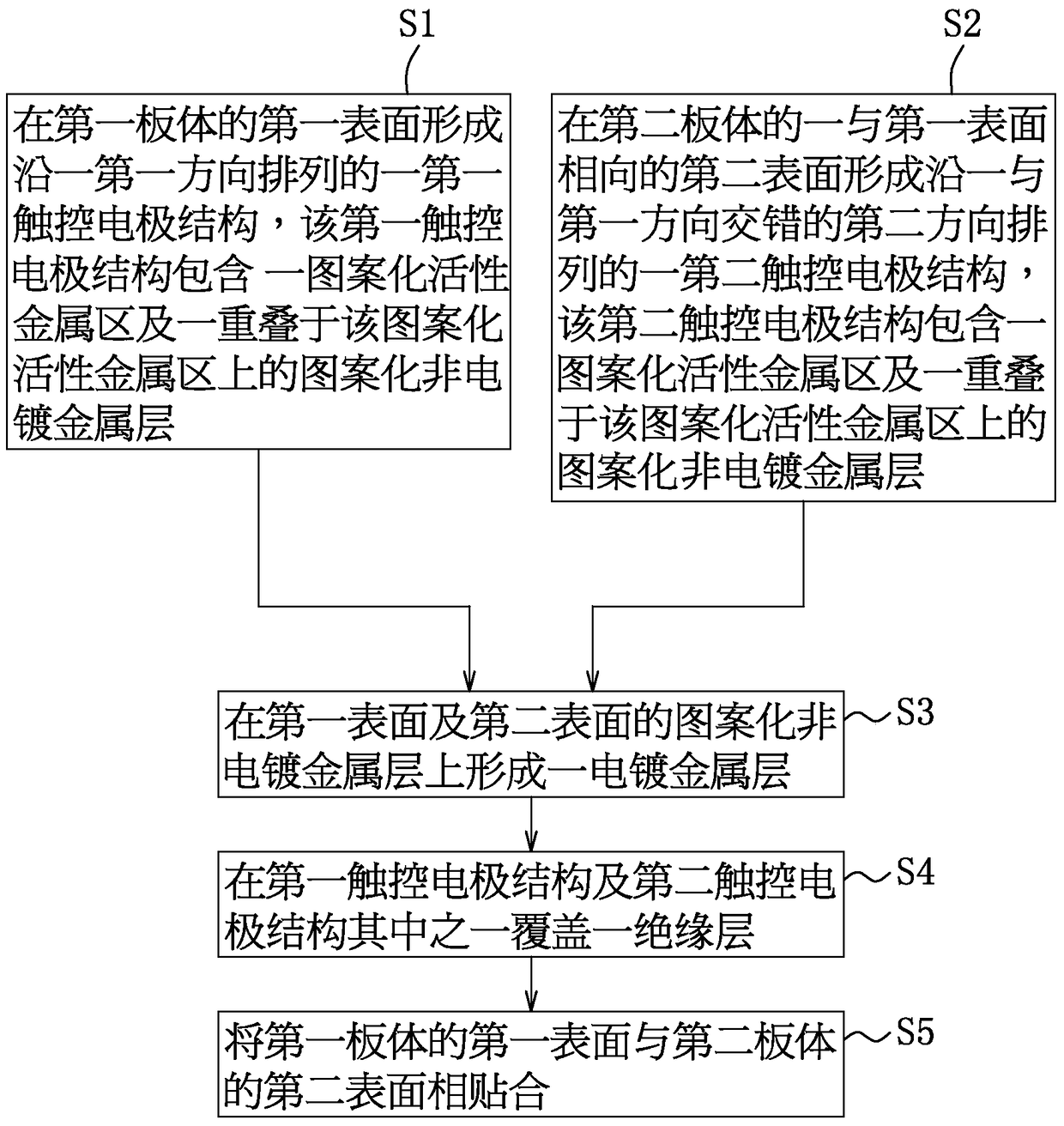
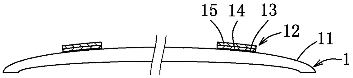
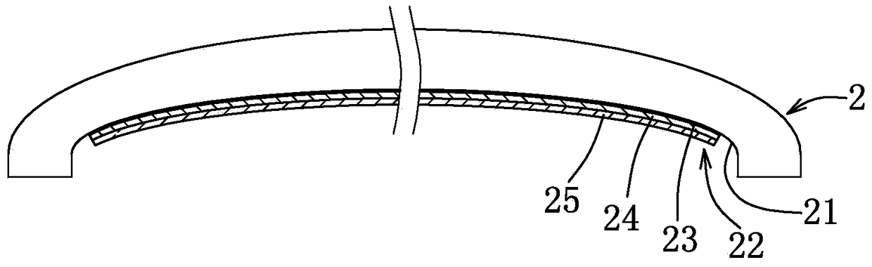
[0042] see figure 1 Shown is the flow chart of the first preferred embodiment of the manufacturing method of the housing with a two-dimensional circuit structure of the present invention, and as figure 2 and image 3 As shown, the housing of this embodiment has a first plate body 1 and a second plate body 2 which are insulated and fitted together, wherein the first plate body 1 has a first surface 11 facing the second plate body 2, The second plate body 2 has a second surface 21 facing the first surface 11, and in this embodiment, the first surface 11 is an outer curved surface, and the second surface 21 is an inner curved surface matching the first surface 11, Instead, it can be attached to the first surface 11 .

[0043] and see figure 1 Steps S1, S2 and cooperate with figure 2 , image 3 In this embodiment, firstly, the first touch electrod...


PUM


Abstract

A touch sensitive housing includes an insulator housing and conductive first and second touch sensor layers formed on the insulator housing, stacked one over the other and insulated from each other. At least one of the first and second touch sensor layers includes a patterned seed sub-layer including a catalytically active metal useful for activating electroless plating and a base sub-layer of a base metal formed on the seed sub-layer and having structural characteristics indicative of the base sub-layer being formed by electroless plating techniques.

Description

technical field [0001] The invention relates to a shell with conductive lines, in particular to a shell with a two-dimensional line structure and a manufacturing method thereof. Background technique [0002] The touch circuit of the existing planar capacitive touch panel can use exposure, development, etching and other processes to stack transparent conductive materials, such as indium tin oxide (ITO), on the surface of a transparent substrate layer by layer to become a transparent capacitive touch panel. plate. The touch circuit can also be a flexible circuit board, which can be directly attached to a substrate to become a non-transparent capacitive touch panel. [0003] And in order to cooperate with the current electronic product housing with a curved surface design, the touchpad needs to be designed as a curved surface so as to fit on an operating curved surface of the electronic product housing. Therefore, Taiwan Patent No. I360073 discloses a manufacturing method of ...

Claims


Application Information

Patent Timeline
Patent Type & Authority Patents(China)
IPC IPC(8): H05K5/02G06F3/044
CPCG06F3/0445G06F2203/04103
Inventor 易声宏廖本逸简槐良
Owner TAIWAN GREEN POINT ENTERPRISE
Why Eureka
Try Eureka