Method for manufacturing flexible substrate and substrate structure

A flexible substrate and flexible technology, applied in semiconductor/solid-state device manufacturing, electrical components, electrical solid-state devices, etc., can solve the problems of high cost of coating raw materials and peeling methods, damage to the internal structure of flexible substrates, and high stress on flexible substrates. Achieve the effect of low raw material cost and operating cost, ensure stability, and avoid offset

Inactive Publication Date: 2015-09-16
TCL CHINA STAR OPTOELECTRONICS TECH CO LTD
View PDF8 Cites 7 Cited by
  • Summary
  • Abstract
  • Description
  • Claims
  • Application Information

AI Technical Summary

Problems solved by technology

[0005] However, the above method has the following defects: First, when the flexible substrate is peeled off, if the peeling strength of the adhesive is too high, the stress on the flexible substrate will b

Method used


Image

  • Method for manufacturing flexible substrate and substrate structure
  • Method for manufacturing flexible substrate and substrate structure
  • Method for manufacturing flexible substrate and substrate structure

Examples


Example Embodiment

[0034] The present invention will be further described below in conjunction with the drawings.

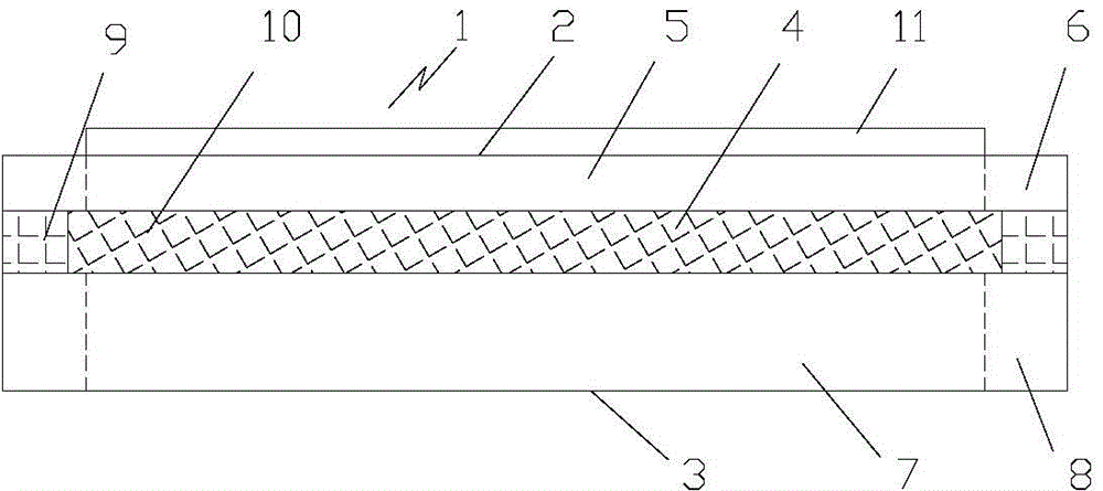
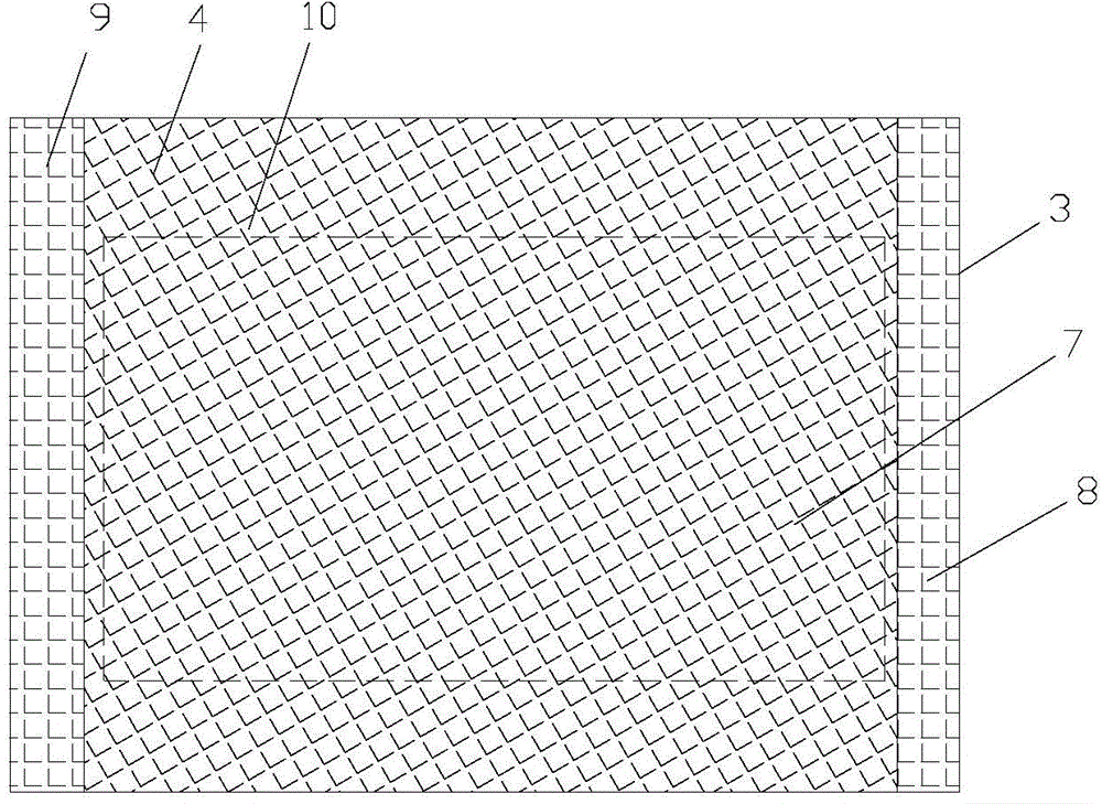
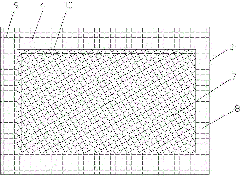
[0035] figure 1 The structure of substrate structure 1 is shown. Such as figure 1 As shown, the substrate structure 1 includes a flexible mother board 2, a rigid mother board 3 and an adhesive layer 4. The flexible mother board 2 has a first effective area 5 forming a flexible substrate and a first inactive area 6 located at the periphery of the first effective area 5. in figure 1 In the middle, the dotted line indicates the boundary between the first effective area 5 and the first non-effective area 6. Correspondingly, the rigid motherboard 3 has a second effective area 7 and a second ineffective area 8, and the second effective area 7 corresponds to the first effective area 5, and the second ineffective area 8 corresponds to the first ineffective area. 8. Similarly, the dashed line represents the boundary between the second effective area 7 and the second non-effective area 8. T...


PUM


Abstract

The invention provides a method for manufacturing a flexible substrate and a substrate structure. The method comprises: 1) providing a rigid motherboard and a flexible motherboard, wherein a second active region of the rigid motherboard is corresponding to a first active region of the flexible motherboard, and a second non-active region of the rigid motherboard is corresponding to a first non-active region of the flexible motherboard; 2)disposing an adhesive layer on the rigid motherboard, wherein the adhesive layer comprises a strong adhesive layer and a weak adhesive layer, the strong adhesive layer is disposed on at least a part of the second non-active region, and the weak adhesive layer is disposed on the other part of the second non-active region and the second active region; 3) covering the adhesive layer with the flexible motherboard through adhering; and 4) cutting the flexible motherboard along an edge of the first active region. The method enables the flexible motherboard to be subjected to a smaller stress during peeling, thus protecting the internal part of the flexible substrate from being damaged.

Description

technical field [0001] The present invention relates to the field of flexible display technology, in particular to a method for manufacturing a flexible substrate and a substrate structure. Background technique [0002] Flexible display refers to a type of display device or display technology that uses flexible substrates and can be manufactured into ultra-thin, ultra-large, and bendable display devices. Flexible display has incomparable advantages over flat panel display, and is a very promising display technology. Through years of scientific research and development, flexible display technology has developed rapidly. [0003] At present, flexible substrates are characterized by thinness, lightness, and flexibility. Therefore, in the production process, the flexible substrate is generally attached to the hard substrate, and the flexible substrate is formed after shaping, and then peeled off after the device manufacturing process is completed. [0004] In the prior art, t...

Claims


Application Information

Patent Timeline
IPC IPC(8): H01L21/50H01L27/15
Inventor 何超
Owner TCL CHINA STAR OPTOELECTRONICS TECH CO LTD
Why Eureka
Try Eureka