Radio frequency sensor and impedance matching device

A technology of radio frequency sensor and radio frequency transmission, applied in semiconductor/solid-state device manufacturing, semiconductor/solid-state device testing/measurement, electrical components, etc. Matching range and matching effect, improving service life, and increasing the effect of process window

Active Publication Date: 2015-09-23
BEIJING NAURA MICROELECTRONICS EQUIP CO LTD
View PDF6 Cites 9 Cited by
  • Summary
  • Abstract
  • Description
  • Claims
  • Application Information

AI Technical Summary

Problems solved by technology

[0007] Since the load impedance of the induction coil 14 is usually at an open point when the RF power supply 24 outputs low-frequency RF power, the current on the transmission line of the RF power supply 24 will be very small. In this case, the impedance matching device 17 starts from the open circuit point Matched, this just can't be detected when the low frequency radio frequency power exists, thus the sensitivity of the radio frequency sensor is not high, thereby can not work because the radio frequency sensor 20 mistakenly judges that the low frequency radio frequency power does not exist, and then causes the impedance matching device 17 to be in the low frequency radio frequency Impedance matching is not performed when the power exists, so the existing impedance matching device is only suitable for matching the RF power within a certain frequency range, resulting in a narrow matching range and poor matching effect of the impedance matching device, which in turn leads to poor pre-cleaning process narrow window
[0008] In order to solve the problem that the sensitivity of the above-mentioned radio frequency sensor is not high, by changing the relevant parameter values ​​of the radio frequency sensor 20, so that when the load impedance of the induction coil 14 is at the open point, it can still be determined that the low frequency radio frequency power exists, thereby avoiding the radio frequency sensor Misjudgment occurs at 20, but this will cause the radio frequency sensor 20 to determine that the determination conditions for the absence of low-frequency radio frequency power are very strict, so that once there are interference factors such as temperature or electromagnetics, even if the low-frequency radio frequency power does not exist, the sensor 20 is also very easy. It is misjudged that it still exists, and then the actuator 22 and the variable elements in the matching network 23 malfunction, resulting in a reduction in the service life of the impedance matching device

Method used


Image

  • Radio frequency sensor and impedance matching device
  • Radio frequency sensor and impedance matching device
  • Radio frequency sensor and impedance matching device

Examples


Embodiment Construction

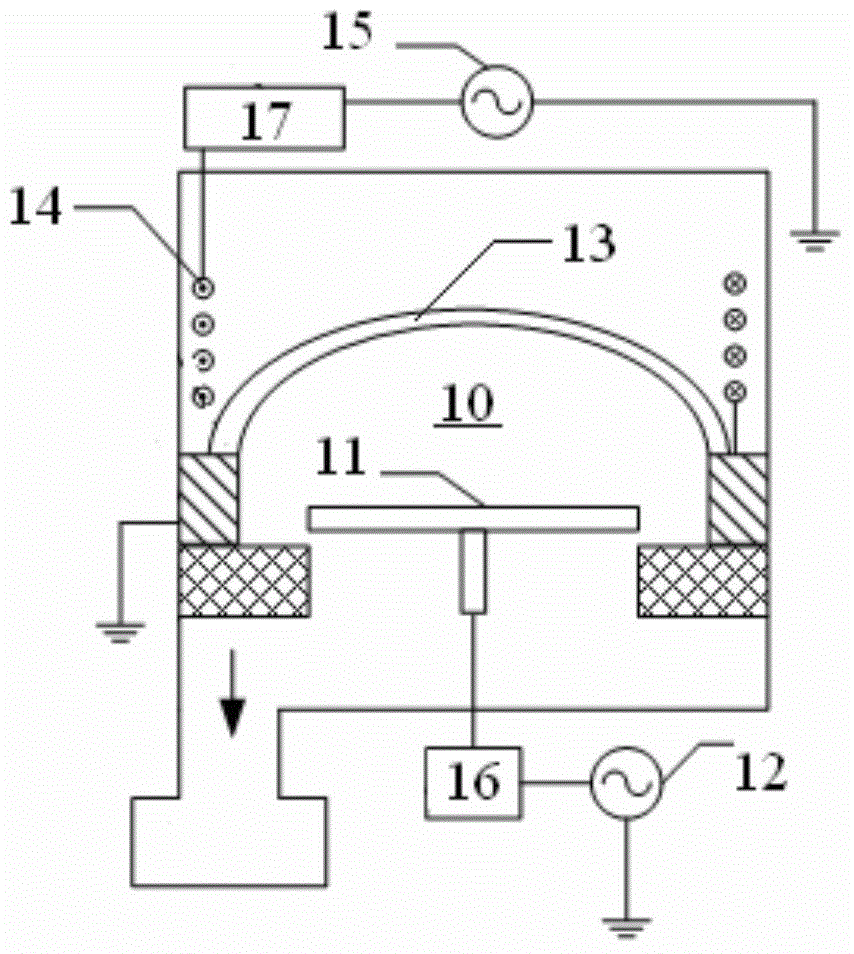
[0028] In order for those skilled in the art to better understand the technical solution of the present invention, the radio frequency sensor and the impedance matching device provided by the present invention will be described in detail below with reference to the accompanying drawings.

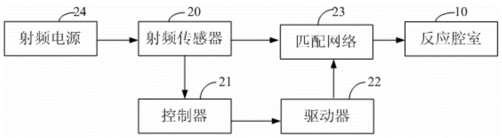
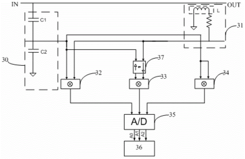
[0029] image 3 A schematic structural diagram of a radio frequency sensor provided by an embodiment of the present invention. see image 3 The radio frequency sensor provided in this embodiment is used to detect the presence of low frequency radio frequency power according to the voltage and current signals on the radio frequency transmission line, and the radio frequency sensor includes a voltage acquisition module 30, a current acquisition module 31, a first analog multiplier 32, a second An analog multiplier 33 , a third analog multiplier 34 , an analog-to-digital conversion module 35 , a control module 36 and a phase shift module 37 . Among them, such as image 3 As shown, the voltag...


PUM


Abstract

The invention provides a radio frequency sensor and an impedance matching device. A voltage acquisition module sends a voltage signal to a first simulation multiplier, one end of a phase shift module and two ends of a third simulation multiplier. A current acquisition module sends a current signal to the first simulation multiplier and the other end of the phase shift module. A voltage and current signal output from the phase shift module is conveyed to two ends of a second simulation multiplier. Through operations of the first simulation multiplier, the second simulation multiplier and the third simulation multiplier, three simulation signals related to the voltage and the current are converted by an analog-to-digital conversion module so as to output digital signals A0, A1 and A2. A control module calculates differential signal values of |delta A0|, |delta A1| and |delta A2| according to the digital signals A0, A1, A2, A0 (0), A1(0) and A2(0). According to the |delta A0|, the |delta A1| and the |delta A2|, low-frequency radio frequency power existence is determined. Sensitivity of the radio frequency sensor, a matching scope and a matching effect of the impedance matching device are increased and mismatching of the impedance matching device is avoided.

Description

technical field [0001] The invention belongs to the technical field of semiconductor processing, and in particular relates to a radio frequency sensor and an impedance matching device. Background technique [0002] Physical vapor deposition (Physical Vapor Deposition, hereinafter referred to as PVD) equipment is a widely used plasma processing equipment, which is mainly used to deposit thin films on the surface of substrates and other processed workpieces. In practical applications, in order to improve the process quality of depositing thin films on the substrate surface, it is often necessary to perform a pre-cleaning process on the processed workpiece before depositing thin films to remove non-volatile impurities on the substrate surface. [0003] figure 1 It is a structural schematic diagram of a pre-cleaning chamber for completing the pre-cleaning process. see figure 1 , the reaction chamber 10 is provided with a carrier device 11 for carrying the substrate, the carri...

Claims


Application Information

Patent Timeline
Patent Type & Authority Applications(China)
IPC IPC(8): H01L21/66
CPCH01L21/67028
Inventor 刘建生
Owner BEIJING NAURA MICROELECTRONICS EQUIP CO LTD
Why Eureka
Try Eureka