Alignment mark and its alignment method

A technology for aligning marks and markings, applied to electrical components, electrical solid devices, circuits, etc., can solve problems affecting lithography accuracy and device yield, and can not take into account the alignment effect, so as to improve lithography accuracy and device yield rate effect

Active Publication Date: 2017-11-14
SEMICON MFG INT (SHANGHAI) CORP +1
View PDF4 Cites 2 Cited by
  • Summary
  • Abstract
  • Description
  • Claims
  • Application Information

AI Technical Summary

Problems solved by technology

However, this does not take into account the alignment effect with the multilayer structure, which affects the lithography accuracy and device yield

Method used


Image

  • Alignment mark and its alignment method
  • Alignment mark and its alignment method
  • Alignment mark and its alignment method

Examples


Embodiment Construction
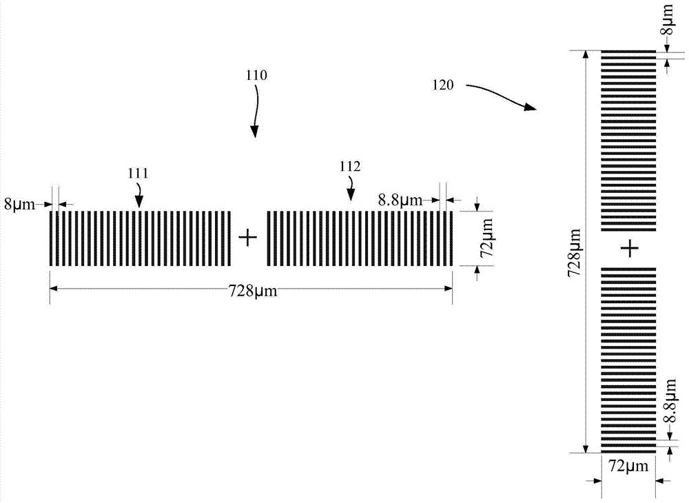
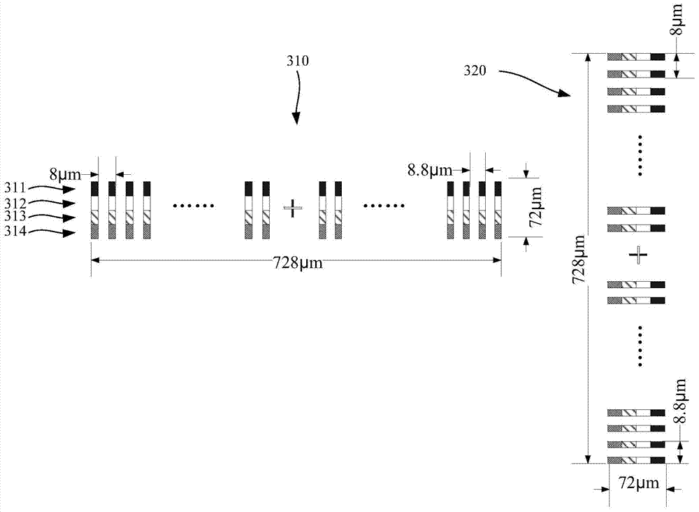
[0022] The core idea of ​​the present invention is to provide an alignment mark and its alignment method. The alignment mark is composed of multiple groups of sub-marks formed in different layers. The main mark composed of the multiple groups of sub-marks is the same as the standard Scribe main mark (SPM) has the same structure, and the standard alignment method can be used to align with the multi-layer structure at one time, so that it can be aligned with multiple layers at the same time.

[0023] The alignment mark and its alignment method proposed by the present invention will be further described in detail below with reference to the drawings and specific embodiments. Advantages and features of the present invention will be apparent from the following description and claims. It should be noted that the drawings are all in a very simplified form and use imprecise ratios, which are only used to facilitate and clearly assist the purpose of illustrating the embodiments of the ...


PUM


Abstract

The invention discloses an alignment mark and its alignment method. The alignment mark includes a set of main marks formed on a semiconductor substrate, the main mark is composed of N groups of sub-marks, and the N groups of sub-marks Formed in N layers of film layers on the substrate, N is the number of layers that need to be aligned in this photolithography process; each group of sub-marks includes the first sub-mark in the horizontal direction and the second sub-mark in the vertical direction; the The first sub-marks are two groups of gratings in the horizontal direction, and the second sub-marks are two groups of gratings in the vertical direction. In this way, it can be aligned with multiple layers during alignment, thereby improving photolithographic precision and device yield.

Description

technical field [0001] The invention relates to the field of integrated circuit manufacturing, in particular to an alignment mark and an alignment method thereof. Background technique [0002] In the manufacture of semiconductor integrated circuits, it is necessary to sequentially transfer the patterns on different masks to the substrate and each film layer of the substrate through lithography equipment to form circuits or micro devices. As the technology develops to smaller dimensions, the precision requirements for photolithography process alignment are getting higher and higher. [0003] There are various alignment methods and alignment marks in the lithography process, among which the scribe lane primary mark (SPM, Scribe lanePrimary Mark) is often used for the alignment between the lithography layer and the layer, usually SPM is used in this lithography process Formed in the scribe lane (Scribe lane), the photolithography process of the subsequent layer is aligned with...

Claims


Application Information

Patent Timeline
Patent Type & Authority Patents(China)
IPC IPC(8): H01L23/544H01L21/66
Inventor 舒强
Owner SEMICON MFG INT (SHANGHAI) CORP
Why Eureka
Try Eureka