Supercharge Your Innovation With Domain-Expert AI Agents!

Display device

A technology for display devices and insulating layers, applied in electrical components, electrical solid devices, circuits, etc., can solve the problems of inability to suppress interlayer peeling, weakening adhesion, and interlayer peeling.

Active Publication Date: 2015-09-30
JAPAN DISPLAY INC
View PDF6 Cites 5 Cited by
  • Summary
  • Abstract
  • Description
  • Claims
  • Application Information

AI Technical Summary

Problems solved by technology

However, even if the concave-convex surface is formed in each layer, since the adjacent layer itself does not change in the laminated film, there is no change in the adhesion between the layer located below and the layer laminated above it, so it may not be possible to suppress the layer. Stripping
[0009] In addition, in the display device using the above-mentioned conventional light-emitting elements, if the uneven surface is to be formed on a plurality of layers arranged on the convex structure, the surface unevenness becomes smaller due to the thickness of the lower layer as the upper layer goes up, and the uneven surface becomes smaller due to the thickness of the lower layer. Planarization of the surface weakens the adhesion between adjacent layers in the stacking direction, which may cause interlayer delamination

Method used


Image

  • Display device
  • Display device
  • Display device

Examples


no. 1 approach

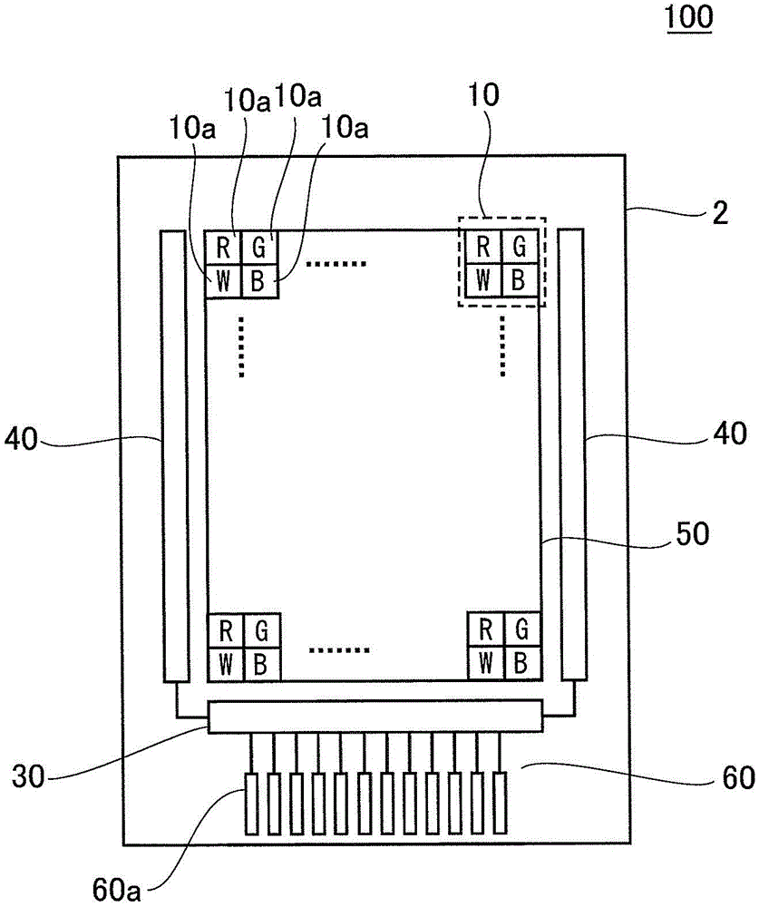
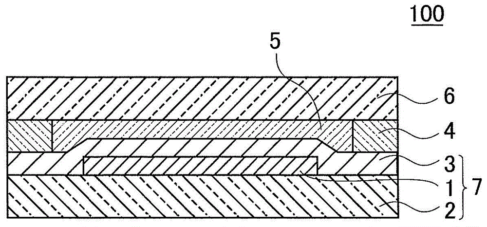
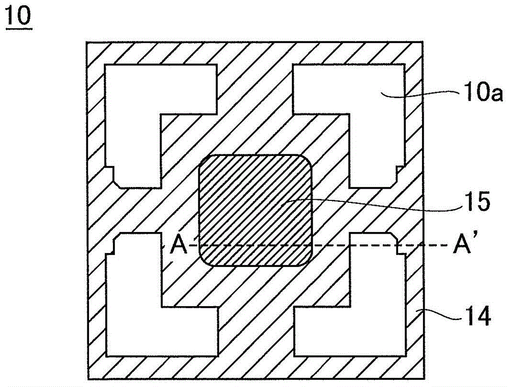
[0038] refer to Figure 3A , Figure 3B , Figure 4A and Figure 4B The display device 100 according to the first embodiment of the present invention will be described.

[0039] Figure 3A and Figure 3B A schematic configuration of the pixel 10 included in the display device 100 according to the first embodiment of the present invention is shown. Figure 3A is the top view of Pixel 10, Figure 3B Yes Figure 3A A cross-sectional view along line A-A' is shown. Figure 4A It is a diagram showing a schematic configuration of a pixel 10 included in the display device 100 according to the first embodiment of the present invention, and shows a plan view of the pixel 10 and a cross-sectional view of the pixel 10 in association. Figure 4B is a cross-sectional view showing a schematic configuration of a pixel 10 included in the display device 100 according to the first embodiment of the present invention, and is Figure 4A An enlarged cross-sectional view of the portion encl...

no. 2 approach

[0065] Hereinafter, a display device 100 according to a second embodiment of the present invention will be described with reference to FIG. 7 .

[0066] 7 is a diagram showing a schematic configuration of a pixel 10 included in a display device 100 according to a second embodiment of the present invention, (a) is a plan view of the pixel 10, and (b) is a line C-C' shown in (a). Sectional view.

[0067] As shown in FIG. 7(a), the pixel 10 included in the display device 100 according to the second embodiment of the present invention may have the following features as the pixel 10 included in the display device 100 according to the first embodiment of the present invention. Structure: The four sub-pixels 10a having a substantially L-shaped light emitting region are respectively arranged at the corners of the rectangular pixel 10 so as to match the substantially L-shaped corners of the light emitting region. In addition, the pixel 10 included in the display device 100 according t...


PUM


Abstract

A display device is provided including a first substrate provided with a pixel, the pixel being provided with a light emitting region of a light emitting device formed by stacking a first electrode, a light emitting layer and second electrode in this order, a first insulating layer having an opening exposing the first electrode at a position corresponding to the light emitting region and provided above the first electrode, a second insulating layer having a certain thickness provided over the first insulating layer and outer region of the opening, and a sealing film provided covering the light emitting device above the second electrode.

Description

technical field [0001] The present invention relates to a display device using a light emitting element. Background technique [0002] An organic electroluminescence element using an organic electroluminescence material (hereinafter also referred to as a "light-emitting element") can emit white light by selecting an organic material or by setting the structure of the light-emitting element to an appropriate structure. The visible light band realizes the emission of each color. Therefore, the development of display devices and lighting fixtures using light-emitting elements has progressed. [0003] A display device using a light-emitting element includes a light-emitting element in each pixel, the light-emitting element of each pixel is connected to a transistor, and light emission is controlled by the transistor. A light emitting element is formed on an element substrate on which transistors are formed. The display device comprises a pixel array in which pixels are arrang...

Claims


Application Information

Patent Timeline
Patent Type & Authority Applications(China)
IPC IPC(8): H01L27/32
CPCH01L27/3213H01L51/5234H01L27/3246H01L27/3258H01L51/5253H10K59/805H10K59/873H10K59/80524H10K59/124H10K50/828H10K50/844H10K59/122H10K59/351
Inventor 森田壮臣仓永卓英奥规夫
Owner JAPAN DISPLAY INC
Features
  • R&D
  • Intellectual Property
  • Life Sciences
  • Materials
  • Tech Scout
  • Unparalleled Data Quality
  • Higher Quality Content
  • 60% Fewer Hallucinations
Learn More