Dummy metal fill shapes for improved reliability of hybrid oxide/low-k dielectrics

a hybrid oxide/low-k dielectric and fill shape technology, applied in the direction of individual semiconductor device testing, semiconductor/solid-state device testing/measurement, instruments, etc., can solve the problems of no known method to increase the strength and robustness of the structure, fill shape does not prevent delamination or add strength, and the effect of preventing undue stresses or delamination

Inactive Publication Date: 2006-06-08
GLOBALFOUNDRIES INC
View PDF16 Cites 21 Cited by
  • Summary
  • Abstract
  • Description
  • Claims
  • Application Information

AI Technical Summary

Benefits of technology

[0011] In a first aspect of the invention, a semiconductor structure is formed on a substrate. The structure includes a first and second rigid dielectric layer and a first non-rigid dielectric wiring level between such layers. The non-rigid layer includes at least one interconnect. A structural securing means is associated with the non-rigid dielectric wiring level for preventing a portion of the first or second rigid dielectric layers adjacent the interconnect from de-layering away from the interconnect and for preventing undue stresses or delamination of via / metal interfaces. In one aspect, the structural securing means are dummy fill shapes in proximity to the interconnect which have a coefficient of thermal expansion substantially the same as the first and second rigid dielectric layer. In one aspect, the dummy fill shapes improve the mechanical stability of the structure relative to the dielectric.
[0012] In another aspect of the invention, the semiconductor structure includes a first rigid dielectric layer a second rigid dielectric layer and a first non-rigid low-k dielectric layer formed between the first and second rigid dielectric layer. A plurality of dummy fill shapes are formed in the first non-rigid layer which replace portions of the first non-rigid low-k dielectric layer with lower coefficient of thermal expansion (CTE) metal such that an overall CTE of the non-rigid low-k dielectric layer and the plurality of dummy fill shapes better matches a CTE of the first and second rigid dielectric layer.
[0013] In still a further aspect of the invention, a structure includes a substrate and at least one front-end-of-line (FEOL) device formed on the substrate. A first rigid layer comprising a dielectric is formed on the at least one FEOL device. A first non-rigid layer comprising a low-k dielectric siloxane based semi-organic layer is formed on the first rigid layer and a second rigid layer comprising a dielectric is formed on the first non-rigid layer. A second non-rigid layer comprising a low-k dielectric is formed on the second rigid layer and a third rigid layer is formed on the second non-rigid layer. At least one interconnect is formed in the second non-rigid layer extending between the second and third rigid layer. At least one dummy fill shape is formed in the second non-rigid layer extending between the second and third rigid layer. The at least one dummy fill shape is composed of an alloy having a coefficient of thermal expansion (CTE) that better matches a CTE of the second and third rigid layer such that the at least one dummy fill shape prevents a portion of the second and the third rigid layers adjacent the interconnect from de-layering away from the interconnect.
[0014] In still another aspect of the invention, a process is provided for forming a semiconductor structure. The process includes forming a first rigid dielectric layer on a substrate and forming a first non-rigid dielectric wiring level on the first rigid dielectric layer having an interconnect. A second rigid dielectric layer is formed on the first non-rigid dielectric wiring level and a plurality of dummy metal fill shapes are formed in the first non-rigid dielectric wiring level in proximity to the interconnect. The dummy metal fill shapes prevent a portion of the first or second rigid dielectric layers adjacent the interconnect from de-layering away from the interconnect.

Problems solved by technology

Any interconnect / via connections in these edge regions are susceptible to resistance shifts and via opens due to repeated deflections from thermal cycling during manufacture, reliability stressing, and use.
Currently, there are no known methods to increase the strength and robustness of the structure.
These dummy fill shapes do not prevent delamination or add strength to the structure as evidenced by the placement of these structures within the interconnect layer.
For example, it is known that dummy fill shapes, as they are presently used in the industry, are deliberately placed away from any metal lines due to the relative difficulty in obtaining the proper manufacturing tolerances.
This, of course, could not then provide any additional strength to the structure.

Method used


Image

  • Dummy metal fill shapes for improved reliability of hybrid oxide/low-k dielectrics
  • Dummy metal fill shapes for improved reliability of hybrid oxide/low-k dielectrics
  • Dummy metal fill shapes for improved reliability of hybrid oxide/low-k dielectrics

Examples


Embodiment Construction

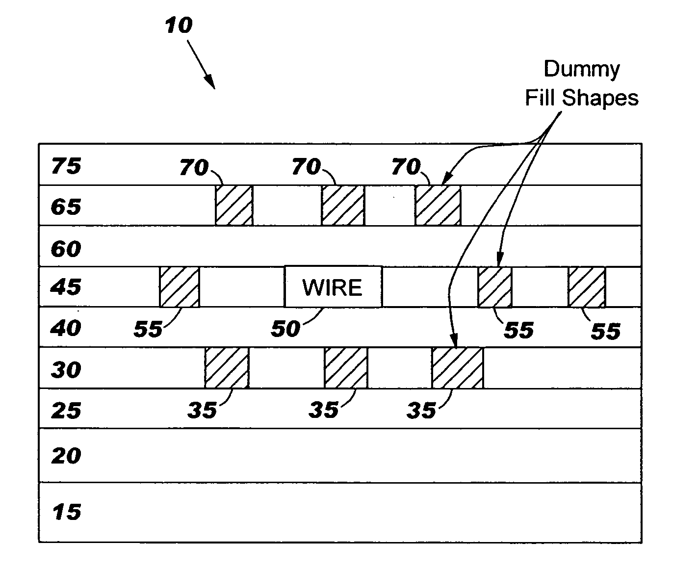
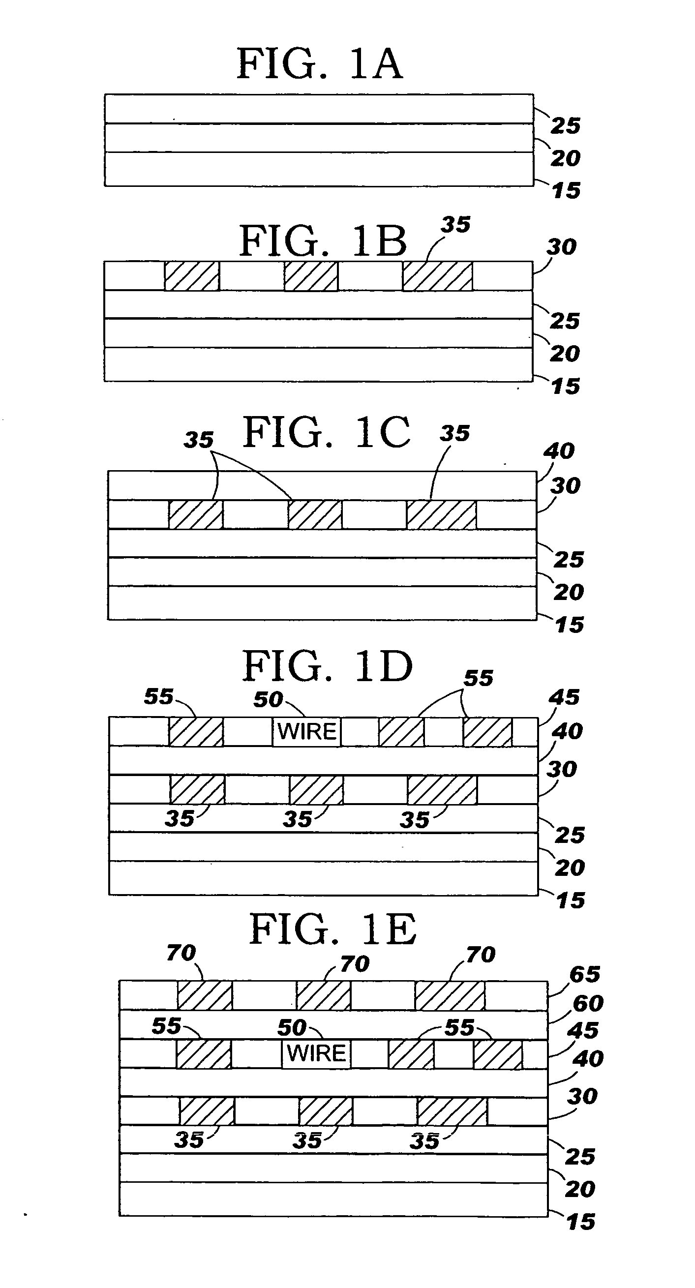
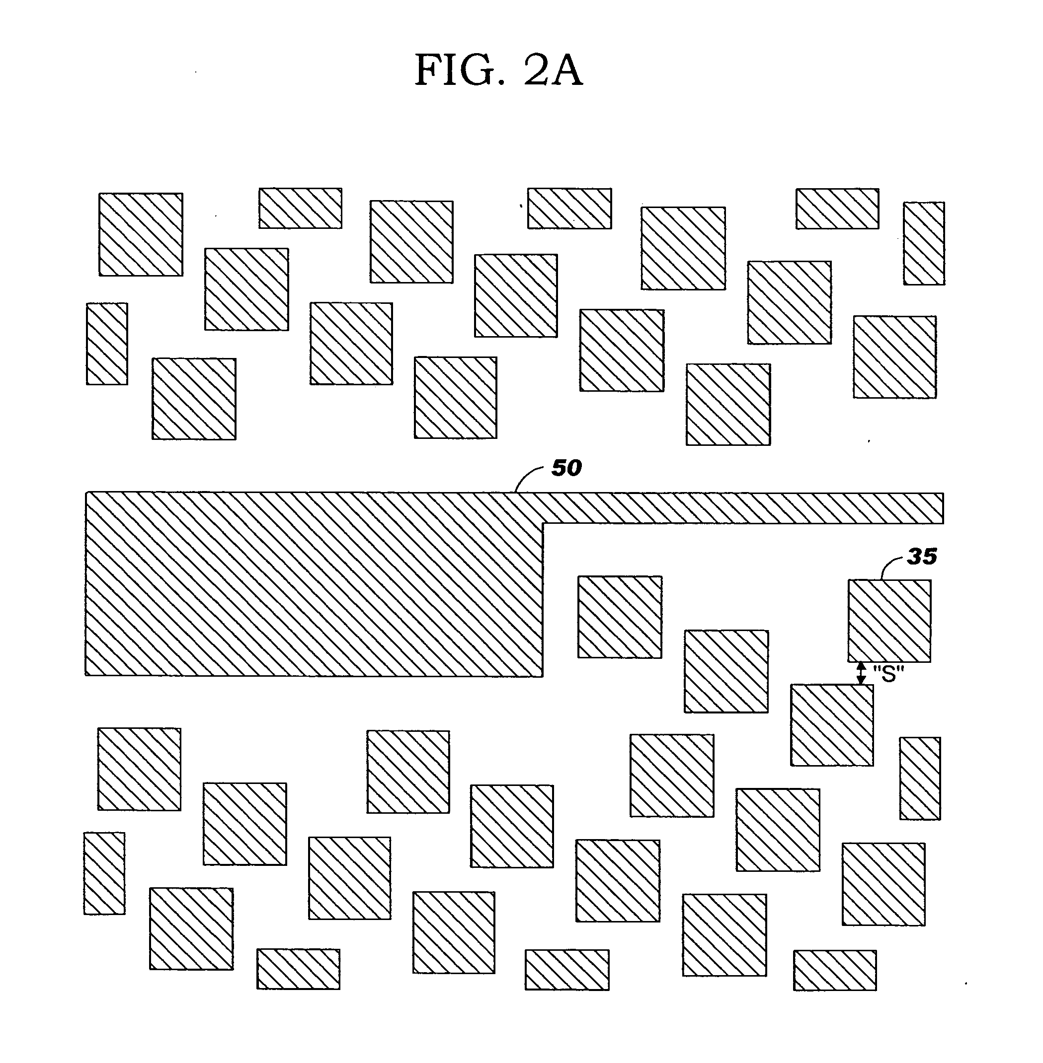
[0019] This invention is directed to a semiconductor device and method of manufacture for preventing de-layering of an adjacent oxide layer away from an interconnect. The invention, in one aspect, uses dummy fill shapes to provide a solution to the problem of locally-high stresses and deflections near metallization structures bounding regions initially devoid of metal shapes. This is accomplished by replacing portions of the high coefficient of thermal expansion material (CTE) / low-k material with relatively low CTE metal such as copper. In this manner, the effective CTE of the region is reduced in proportion to the density of the dummy metal fill shapes. It has also been found that the use of the dummy fill shapes improve the mechanical stress and stiffness of the structure since they tend to adhere between the upper and lower dielectric layers. A benefit that is derived from the invention is significantly improved reliability and robustness of the interconnects.

[0020] By use of th...


PUM

PropertyMeasurementUnit
widthaaaaaaaaaa
widthaaaaaaaaaa
widthaaaaaaaaaa

Abstract

Semiconductor structure including a first rigid dielectric layer and a second rigid dielectric layer. A first non-rigid low-k dielectric layer is formed between the first and second rigid dielectric layer. A plurality of dummy fill shapes is formed in the first non-rigid layer which replace portions of the first non-rigid low-k dielectric layer with lower coefficient of thermal expansion (CTE) metal such that an overall CTE of the first non-rigid low-k dielectric layer and the plurality of dummy fill shapes matches a CTE of the first and second rigid dielectric layers more closely than that of the first non-rigid low-k dielectric layer alone.

Description

CROSS REFERENCE TO RELATED APPLICATIONS [0001] The present application is a divisional of U.S. application Ser. No. 10 / 605,891 filed Nov. 4, 2003, the disclosure of which is expressly incorporated by reference herein in its entirety, which, in turn, claims priority of U.S. provisional application Ser. No. 60 / 320,074, filed on Apr. 1, 2003, which is incorporated herein in its entirety.BACKGROUND OF INVENTION [0002] 1. Field of the Invention [0003] The invention generally relates to a semiconductor device and method of manufacture and, more particularly, to a semiconductor device and method of manufacture which reduces mismatch driven stresses and deflections between interconnect layers. [0004] 2. Background Description [0005] To fabricate microelectronic semiconductor devices such as an integrated circuit (IC), many different layers of metal and insulation are selective deposited on a silicon wafer. The insulation layers may be, for example, silicon dioxide, silicon oxynitride, fluor...

Claims


Application Information

Patent Timeline
Patent Type & Authority Applications(United States)
IPC IPC(8): H01L23/52H01L23/522
CPCH01L23/522H01L2924/0002Y10T428/12549Y10T428/12542H01L2924/00
Inventor LANDIS, HOWARD S.
Owner GLOBALFOUNDRIES INC
Why Eureka
Try Eureka