Inverted structure of III conductor light-emitting device

一种发光器件、半导体的技术,应用在半导体器件、电固体器件、电气元件等方向,能够解决蚀刻孔洞高、工艺复杂、生产成本高等问题,达到简化制程的效果

Active Publication Date: 2015-09-30
XIANGNENG HUALEI OPTOELECTRONICS
View PDF6 Cites 15 Cited by
  • Summary
  • Abstract
  • Description
  • Claims
  • Application Information

AI Technical Summary

Problems solved by technology

[0002] Traditional light-emitting diodes adopt a front-mount structure. Generally, the transparent conductive layer is made of high-transmittance materials, such as ITO, AZO, etc., and the electrodes are generally made of Cr / Pt / Au, etc. However, in the flip-chip structure, the light excited by the active layer It is directly emitted from the substrate on the other side of the electrode, so the requirement for the P-type electrode is changed to a highly reflective material covering the entire p-type nitride semiconductor layer as a mirror structure. The first is on the p-type nitride semiconductor layer Plating a transparent electrode with high transmittance plus high reflective metal, such as ITO / Ag, etc., the other is to directly coat a high reflective metal on the p-type nitride semiconductor layer as an ohmic contact layer and a mirror, For example, Ag, Al, etc., no matter which method is selected, a metal protective layer (guard metal) must be used later to cover the highly reflective material to avoid instability, and then etch multiple holes (vias). The schematic diagram of the structure is as follows figure 1 , the entire surface is covered with the first insulating layer, the n-type nitride semiconductor layer and the metal protection layer are opened to access the n-type nitride semiconductor layer and the metal protection layer, and then the P-type contact metal and the N-type contact metal are plated, and the entire surface is covered with the second insulating layer, and the hole is accessed to access the P Type contact metal and N-type contact metal, and finally flip-chip P-type electrodes and N-type electrodes are plated. Due to the relatively high precision of etching holes, the process is complicated and the production cost is also high.

Method used


Image

  • Inverted structure of III conductor light-emitting device
  • Inverted structure of III conductor light-emitting device
  • Inverted structure of III conductor light-emitting device

Examples


Embodiment 1

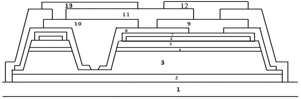
[0060] combine Figure 2a-Figure 13 , an object of the present invention is to provide a novel flip-chip structure of a Group III semiconductor light emitting device, comprising: a substrate 1, a buffer layer 2, an n-type nitride semiconductor layer 3, an active layer 4, a p-type nitride semiconductor Layer 5, first insulating layer structure 8-1, P-type contact metal 9, N-type contact metal 10, second insulating layer structure 11-1, flip-chip P-type electrode 12, flip-chip N-type electrode 13 and transparent conductive layer 14;

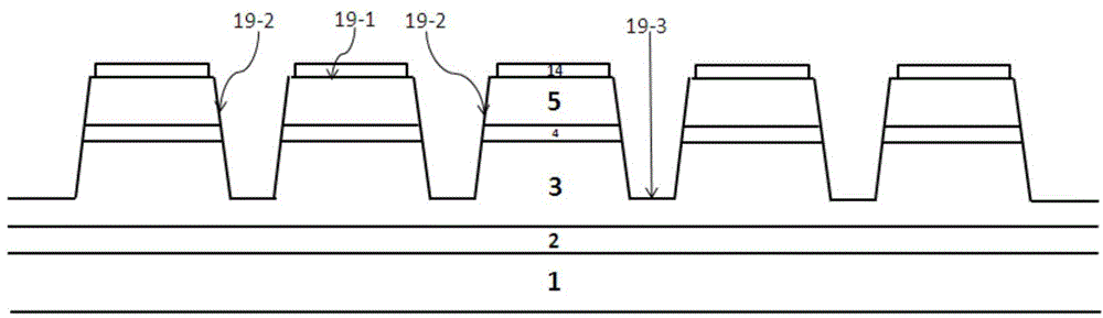
[0061] Wherein, the substrate 1, the buffer layer 2, the n-type nitride semiconductor layer 3, the active layer 4, and the p-type nitride semiconductor layer 5 arranged in sequence from bottom to top form a nitride semiconductor layer with a linear convex mesa 19. structure.

[0062] The linear convex mesa 19: includes a first upper surface 19-1, a side surface 19-2 and a second upper surface 19-3, the first upper surface 19-1 and the second uppe...

Embodiment 2

[0108] The flip-chip structure in this embodiment all adopts the technology of line convex mesa 19 instead of the technology of multiple vias.

[0109] Such as Figure 3a Shown is a top view of a plurality of vias in the prior art, Figure 3b for Figure 3a Sectional view along the A-B direction.

[0110] Such as Figure 4a Shown is a top view of a linear convex table top, Figure 4b for Figure 4a Sectional view along C-D direction.

[0111] The etched area of ​​the line convex mesa 19 is single or multiple lines;

[0112] The substrate 1, the buffer layer 2, the n-type nitride semiconductor layer 3, the active layer 4 and the p-type nitride semiconductor layer 5 form a nitride semiconductor structure with a line convex mesa 19;

[0113] The linear convex mesa includes a first upper surface 19-1, a side surface 19-2 and a second upper surface 19-3, and the two ends of the first upper surface are respectively provided with the side surface and the second upper surface. ...

Embodiment 3

[0116] On the basis of Embodiment 2, the lower end of the P-type wire electrode 15 in this embodiment is arranged on the transparent conductive layer 14 (such as Figure 5a shown) or arranged on the surface of the first insulating layer structure 8-1 and on the transparent conductive layer 14 (such as Figure 5b shown).


PUM

PropertyMeasurementUnit
wavelengthaaaaaaaaaa

Abstract

The invention discloses an inverted structure of an III conductor light-emitting device. The inverted structure comprises a substrate, a buffer layer, an N-type nitride semiconductor layer, an active layer, a P-type nitride semiconductor layer, a transparent conductive layer, a first insulating layer structure, P-type contact metal, N-type contact metal, a second insulating layer structure, an inverted P-type electrode and an inverted N-type electrode. The substrate, the buffer layer, the N-type nitride semiconductor layer, the active layer and the P-type nitride semiconductor layer arranged in order from top to bottom form a linear raised top. The linear raised top replaces the prior multiple vias; the first insulating layer structure, using a Bragg reflector layer-metal layer-single oxide insulating layer or a Bragg reflector layer-metal layer-multiple oxide insulating layers as a reflector structure and insulating layer, replaces the inverted reflector structure and first insulating layer; a metal protective layer can be omitted.

Description

technical field [0001] The present application relates to the technical field of semiconductor lighting, and specifically relates to a flip-chip structure of a Group III semiconductor light emitting device. Background technique [0002] Traditional light-emitting diodes adopt a front-mount structure. Generally, the transparent conductive layer is made of high-transmittance materials, such as ITO, AZO, etc., and the electrodes are generally made of Cr / Pt / Au, etc. However, in the flip-chip structure, the light excited by the active layer It is directly emitted from the substrate on the other side of the electrode, so the requirement for the P-type electrode is changed to a highly reflective material covering the entire p-type nitride semiconductor layer as a mirror structure. The first is on the p-type nitride semiconductor layer Plating a transparent electrode with high transmittance plus high reflective metal, such as ITO / Ag, etc., the other is to directly coat a high reflec...

Claims


Application Information

Patent Timeline
Patent Type & Authority Applications(China)
IPC IPC(8): H01L33/20H01L33/10H01L33/14H01L33/36H01L33/62
CPCH01L33/10H01L33/14H01L33/20H01L33/36H01L33/62H01L27/153H01L33/32H01L33/382H01L33/42H01L33/46H01L25/0756H01L33/38
Inventor 许顺成
Owner XIANGNENG HUALEI OPTOELECTRONICS
Why Eureka
Try Eureka