Method for manufacturing three-dimensional circuit on surface of injection molded part

A technology of three-dimensional circuits and injection molded parts, which is applied in the direction of printed circuits, printed circuit manufacturing, electrical components, etc., can solve the problems of large loss of raw materials, complicated manufacturing process, and serious environmental pollution, and achieve volume and cost reduction, simple process, Reduce the effect of using

Active Publication Date: 2015-09-30
马鞍山塑丞精密制造有限公司
View PDF3 Cites 27 Cited by
  • Summary
  • Abstract
  • Description
  • Claims
  • Application Information

AI Technical Summary

Problems solved by technology

This process can be used to produce three-dimensional circuits on some large injection molded parts, but is not suitable for manufacturing three-dimensional circuits on injection molded parts with complex structures
[0007] The above three traditional metallization methods on the surface of injection molded parts cannot meet the requirements of high-precision and flexible manufacturing due to the complicated manufacturing process, large loss of raw materials, and serious environmental pollution.

Method used


Image

  • Method for manufacturing three-dimensional circuit on surface of injection molded part
  • Method for manufacturing three-dimensional circuit on surface of injection molded part
  • Method for manufacturing three-dimensional circuit on surface of injection molded part

Examples


Embodiment 1

[0029] A method of manufacturing a three-dimensional circuit on the surface of an injection molded part, comprising the steps of:

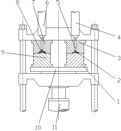
[0030] A. The base layer 15 is formed by injection molding the first layer of base material 2 through the common injection unit 4 of the double-material injection molding machine. The base material 2 of the first base is a common plastic, and the present embodiment selects a mixture of PC and ABS, wherein the Said PC mass percentage is 70%, and said ABS mass percentage is 30%;

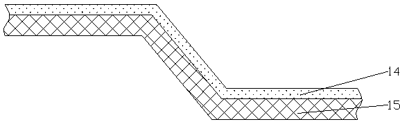
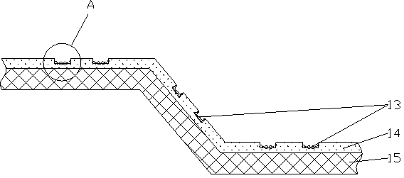
[0031] B. Through the metal powder injection unit 6 and the mold of the double-material injection molding machine, the second layer of compound material 8 is injected onto the upper surface of the base layer 15 to form a metal powder injection layer 14. After cooling under pressure, the mold is opened to take out the injection molded part, and the second layer is mixed. Material 8 is made up of copper powder 13 and non-platable resin binder, and described copper powder 13 ...

Embodiment 2

[0041] A method of manufacturing a three-dimensional circuit on the surface of an injection molded part, comprising the steps of:

[0042] A. A base layer 15 is formed by injection molding the first layer of base material 2 through the common injection unit 4 of the double-material injection molding machine. The base material 2 of the first base is ordinary plastic, and PC is selected in this embodiment;

[0043] B. Through the metal powder injection unit 6 and the mold of the double-material injection molding machine, the second layer of compound material 8 is injected onto the upper surface of the base layer 15 to form a metal powder injection layer 14. After cooling under pressure, the mold is opened to take out the injection molded part, and the second layer is mixed. Material 8 is composed of copper powder 13 and non-platable resin binder, the size of the copper powder 13 is 220 mesh, and the mass percentage of 8 in the second layer of mixed material is 88%, and the volume...

Embodiment 3

[0048] A method of manufacturing a three-dimensional circuit on the surface of an injection molded part, comprising the steps of:

[0049] A. Form the matrix layer 15 through the ordinary injection unit 4 of the double-material injection molding machine and the first layer of matrix material 2 through the mold injection molding. The first layer of matrix material 2 is ordinary plastic, and ABS is selected in this embodiment;

[0050] B. Through the metal powder injection unit 6 and the mold of the double-material injection molding machine, the second layer of compound material 8 is injected onto the upper surface of the base layer 15 to form a metal powder injection layer 14. After cooling under pressure, the mold is opened to take out the injection molded part, and the second layer is mixed. Material 8 is made up of copper powder 13 and non-platable resin binder, and the size of described copper powder 13 is 250 mesh, and the mass percentage of 8 in the second layer of mixed m...


PUM


Abstract

The invention discloses a method for manufacturing a three-dimensional circuit on a surface of an injection molded part. The method comprises the steps of A. performing injection molding on a substrate layer through a double-material injection molding machine; B. performing injection molding on the upper surface of the substrate layer through the double-material injection molding machine for forming a metal powder injection-molded layer,, performing pressure-keeping cooling, and opening a mold for taking the injection molded part out; C. performing selective sintering on the metal powder injection molded layer on the surface of the injection molded part through the laser head a CO2 laser in a vacuum environment according to a pre-designed circuit wiring pattern path for forming a primary three-dimensional circuit; and D. performing electroless copper plating on the copper powder which is bared after laser sintering for obtaining an electroless copper-plated layer, thereby forming a copper lead. Relative to a traditional method for manufacturing the three-dimensional circuit, the method of the invention has a simple process and is suitable for high-precision batch production. According to the method of the invention, the three-dimensional circuit can be manufactured on the high-strength injection molded part, and use number of plate type printed circuit boards can be reduced, thereby reducing size and cost of an electronic product and satisfying a requirement for a specific structure.

Description

technical field [0001] The invention relates to a method for manufacturing a three-dimensional circuit, in particular to a method for selectively sintering the surface layer of an injection molded part containing metal copper powder by laser, and obtaining a copper wire by electroless copper plating, thereby manufacturing a three-dimensional circuit on the surface of the injection molded part. Background technique [0002] A three-dimensional circuit is also called a three-dimensional circuit, which refers to the use of certain processing methods on the surface of the injection-molded plastic shell to produce the required graphic wires, and then through the assembly of electronic components, the electrical interconnection of ordinary printed circuit boards Functions such as support, protection and protection of the plastic shell are integrated on one injection molded part to form a three-dimensional circuit carrier. [0003] The traditional methods of generating three-dimens...

Claims


Application Information

Patent Timeline
Patent Type & Authority Applications(China)
IPC IPC(8): H05K3/00B22F3/105C23C18/38
CPCY02P10/25
Inventor 吴松琪刘斌
Owner 马鞍山塑丞精密制造有限公司
Why Eureka
Try Eureka