Golden finger processing method characterized by no lead wire residues

A processing method, gold finger technology, applied in the processing steps sequence, electrical connection formation of printed components, electrical components, etc., can solve problems such as reducing production costs, achieve the effects of reducing production costs, improving yield, and reducing refills

Inactive Publication Date: 2015-10-07
VICTORY GIANT TECH HUIZHOU CO LTD
View PDF5 Cites 5 Cited by
  • Summary
  • Abstract
  • Description
  • Claims
  • Application Information

AI Technical Summary

Problems solved by technology

[0003] In view of this, the technical problem to be solved by the present invention is a gold finger processing method without lead residues that reduces production costs and reduces the rate of defective products

Method used


Image

  • Golden finger processing method characterized by no lead wire residues
  • Golden finger processing method characterized by no lead wire residues
  • Golden finger processing method characterized by no lead wire residues

Examples


Embodiment 1

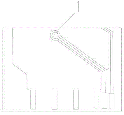
[0030] Such as figure 1 As shown, a gold finger treatment method without lead wire residue comprises the following steps:

[0031] S1. Fabrication, pressing, and drilling of the inner circuit board, and electroplating the entire surface of the outer circuit board to make the outer circuit board.

[0032] S2. The first outer graphics transfer.

[0033] According to the distribution of the golden finger part of the outer circuit board, select the network connection point suitable for the golden finger part. Such as figure 1 As shown, when the network connection point 1 of the golden finger part of the outer circuit board is determined to be between the PAD hole and the copper skin, make a film picture A, and make a graphic of the network connection point in the film picture A. When making the film picture A, the circuit graphics, gold finger parts and network connection points connecting each gold finger are all light-transmitting parts, and other parts are opaque parts. Pas...

Embodiment 2

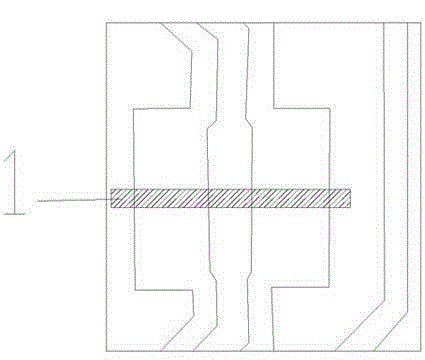
[0044] Such as figure 2 As shown, a gold finger treatment method without lead wire residue comprises the following steps:

[0045] S1. Fabrication, pressing, and drilling of the inner circuit board, and electroplating the entire surface of the outer circuit board to make the outer circuit board.

[0046] S2. The first outer graphics transfer.

[0047] According to the distribution of the golden finger part of the outer circuit board, select the network connection point suitable for the golden finger part. Such as figure 2 As shown, when it is determined that the network connection point 1 of the golden finger part of the outer circuit board is between the patches, make a film picture A, and make a graphic of the network connection point in the film picture A. When making the film picture A, the circuit graphics, gold finger parts and network connection points connecting each gold finger are all light-transmitting parts, and other parts are opaque parts. Paste a layer of ...

Embodiment 3

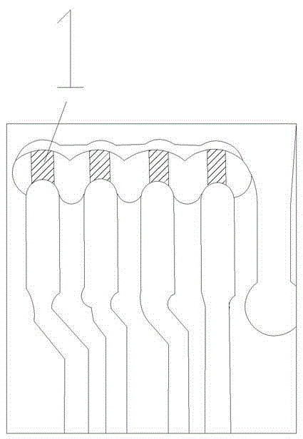
[0058] Such as image 3 As shown, a gold finger treatment method without lead wire residue comprises the following steps:

[0059] S1. Fabrication, pressing, and drilling of the inner circuit board, and electroplating the entire surface of the outer circuit board to make the outer circuit board.

[0060] S2. The first outer graphics transfer.

[0061] According to the distribution of the golden finger part of the outer circuit board, select the network connection point suitable for the golden finger part. Such as image 3 As shown, when it is determined that the network connection point 1 of the gold finger part of the outer circuit board is between the IC and the copper skin, make a film picture A, and make a graphic of the network connection point in the film picture A. When making the film picture A, the circuit graphics, gold finger parts and network connection points connecting each gold finger are all light-transmitting parts, and other parts are opaque parts. Paste ...


PUM


Abstract

The invention discloses a golden finger processing method characterized by no lead wire residues. The method comprises the following steps of (S1) internal circuit board making, laminating and boring, and full-plate electroplating; (S2) external pattern transferring for the first time; (S3) circuit board etching and film stripping; (S4) circuit board appearance detecting; (S5) external pattern transferring for the second time; (S6) hard gold layer electroplating on the golden finger part of the circuit board, and film stripping; (S7) external pattern transferring for the third time; (S8) circuit board etching and film stripping; and (S9) solder mask printing and moulding surface processing to make the circuit board. The golden finger network connection point residues are effectively prevented. Copper exposed on the front of the cut golden finger is also prevented. Phenomena of burring, upwarping during a production process are eliminated. Material supplementing on the golden finger part of the circuit board is reduced during the production process. The workload of workers is reduced. The production efficiency is improved. The generated defective products are reduced. The discarded products are also reduced. The production cost is lowered. The yield is further improved.

Description

technical field [0001] The invention belongs to the technical field of circuit board production, and in particular relates to a gold finger treatment method without lead wire residue. Background technique [0002] At present, the production of outer circuit boards in the PCB circuit board manufacturing industry usually adopts the following process: drilling → removing slag / copper sinking in holes → full board electroplating → image transfer → graphic electroplating → line etching → solder resist oil screen printing → text oil Silk screen printing → surface treatment (gold / silver / tin) → contour processing → final quality control, and finally make a qualified circuit board. However, when the existing circuit board manufacturers perform the electroplating process on the gold fingers, they first add leads to the front end, and then connect the peripheral gold plating wires to achieve gold plating on the fingers. However, there are too many hidden dangers and disadvantages in th...

Claims


Application Information

Patent Timeline
Patent Type & Authority Applications(China)
IPC IPC(8): H05K3/40
CPCH05K3/4007H05K2203/14
Inventor 陈涛赵启祥施世坤张亚锋
Owner VICTORY GIANT TECH HUIZHOU CO LTD
Why Eureka
Try Eureka