

Semiconductor device
A semiconductor, conductive type technology, applied in the direction of semiconductor devices, semiconductor/solid-state device manufacturing, electrical components, etc., can solve problems such as FWD88 damage
- Summary
- Abstract
- Description
- Claims
- Application Information
AI Technical Summary
Problems solved by technology
Method used
Image

Examples
Embodiment 1
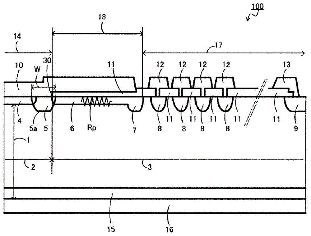
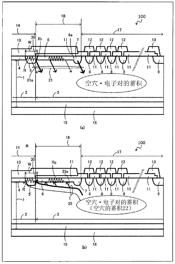
[0072] figure 1 It is a sectional view of main parts of the semiconductor device 100 according to the first embodiment of the present invention. figure 1 is equivalent to Figure 8 The main part cross section of the FWD of FWD88 in the figure shows the main part cross section of the semiconductor device from the vicinity of the edge part of an active part to the outer peripheral part of a semiconductor substrate. figure 1 Among them, the semiconductor device 100 includes the p anode region 4 arranged on the upper surface of the n drift region 2 . The p diffusion region 5 is provided on the n drift region 2 . The p diffusion region 5 is disposed in contact with the p anode region 4 and has a lower concentration than the p anode region 4 and has a deeper diffusion depth. n in the epitaxial part of the n drift region 2 - Region 3 forms edge termination structures 17 and the like.
[0073] in n - On the area 3, there are provided: a resistance area 6 arranged in contact wit...
Embodiment 2
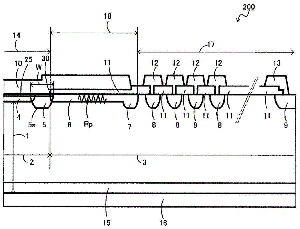
[0094] image 3 It is a cross-sectional view of main parts of a semiconductor device 200 according to Embodiment 2 of the present invention. The difference from Example 1 is that a high-concentration p region 25 (p + ). When the surface concentration of the p-diffusion region 5 is low, ohmic contact with the anode electrode 10 becomes difficult and the contact resistance increases. As the contact resistance increases, the amount of holes trapped from the p diffusion region 5 decreases, and almost all the holes are trapped in the p anode region 4 . As a result, current concentration occurs in the p anode region 4, resulting in damage to the element.
[0095] As a countermeasure to prevent this phenomenon, in order to reduce the contact resistance with the anode electrode 10 while keeping the impurity concentration of the p diffusion region 5 low, it is possible to set the impurity concentration higher than the p diffusion region 5 and the diffusion depth to be lower. Shallo...
Embodiment 3
[0098] Figure 4 It is a sectional view of main parts of a semiconductor device 300 according to Embodiment 3 of the present invention. This semiconductor device 300 differs from Embodiment 1 in the following two points. The first point is: the resistance region 26 is arranged in such a way as to be in contact with the p anode region 4 and the resistance end region 7, that the diffusion depth of the resistance region 26 is deeper than that of the p anode region 4 and the resistance region 6, and is deeper than that of the p anode region 4 and the resistance region 6. The diffusion depth of the guard ring region 8 is shallow. The second point is to separate (shrink) the end of the portion where the p anode region 4 contacts the anode electrode 10 from the resistance region 26 . Figure 4 In the figure, the insulating film 11 is represented by two insulating films of PSG film 11b of phosphorous glass and thermal oxide film 11a.
[0099] The buffer region 18 of Example 3 also ...
PUM
 Abstract
Description
Claims
Application Information