Grid electrode formation method and transistor formation method

A transistor and gate technology, applied in the field of semiconductor manufacturing, can solve problems affecting the performance of semiconductor devices and processes, and achieve the effects of reducing energy, reducing the degree of influence, and reducing the temperature of electrons

Active Publication Date: 2015-10-14
SEMICON MFG INT (SHANGHAI) CORP
View PDF3 Cites 5 Cited by
  • Summary
  • Abstract
  • Description
  • Claims
  • Application Information

AI Technical Summary

Problems solved by technology

[0005] The recesses will shift the positions of the subsequently formed source and drain regions to the bottom of the substrate, thereby affecting the performance of the semiconductor device
In addition, in the subsequent step of forming an interlayer interconnection structure, in order to optimize the contact performance between the source region and the drain region and the subsequently formed metal interconnection line, a silicide layer (silicide layer) may be formed on the surface of the source region and the drain region. ), at this time, the position of the source region and the drain region shifts toward the bottom of the substrate, which means that the silicide layer formed on the source region and the drain region will also shift toward the bottom of the substrate accordingly, which will affect the subsequent process conduct

Method used


Image

  • Grid electrode formation method and transistor formation method
  • Grid electrode formation method and transistor formation method
  • Grid electrode formation method and transistor formation method

Examples


Embodiment Construction

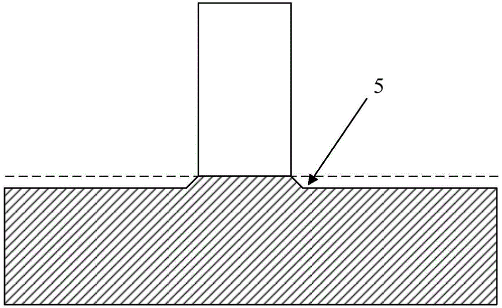
[0044] In the existing process of etching the gate material layer to form the gate, it is easy to cause a certain degree of loss (loss) to the substrate, resulting in recesses (recesses) being formed on the substrate surface on both sides of the formed gate.

[0045] For example, when the etching process is carried out to a certain extent, a part of the substrate will be exposed, and it is easy to cause a certain loss to the substrate at this moment; Penetration into the substrate and consequent loss of the substrate.

[0046] To this end, the present invention provides a method for forming a gate, comprising the following steps: providing a substrate; forming a gate material layer on the substrate; performing plasma etching on the gate material layer to form a gate ; Wherein, the power output by the etching machine is in the form of pulses, and the gate material layer is pulsed etched.

[0047] Through the above steps, the etching machine is made to output pulsed power to pe...


PUM


Abstract

The invention provides a grid electrode formation method and a transistor formation method. The grid electrode formation method comprises steps of providing a substrate; forming a material layer of a grid electrode on the substrate; and performing plasma etching on the material layer of the grid electrode using a plasma etcher, so as to form the grid electrode, wherein the plasma etching comprises a step of enabling the plasma etcher to output pulse-type power so as to perform pulse etching on the material layer of the grid electrode. The invention also provides the transistor formation method. The transistor formation method comprises a step of forming the grid electrode of a transistor using the abovementioned method. The invention has the beneficial effects that etching in the etching mode can achieve a discontinuous etching effect, so that the electron temperature of plasma can be lowered to a certain degree during etching interruption, reduction in the electron temperature of plasma is facilitated, the influence on the substrate is further reduced, that is to say, loss of the substrate is reduced when the grid electrode is formed by etching, and recesses are prevented from being formed in the substrate.

Description

technical field [0001] The invention relates to the field of semiconductor manufacturing, in particular to a method for forming a gate and a transistor. Background technique [0002] In the prior art, it is easy to form recesses on the substrate on both sides of the gate during various steps of forming a semiconductor device. [0003] For example, in the existing process of forming a gate, generally a layer of gate material is covered on the substrate first, and then part of the gate material layer is removed by mask etching, and the remaining gate material remains The layer forms the gate of the semiconductor device. However, in the process of etching the gate material layer, it is often difficult to avoid loss (loss) on the substrate portion. [0004] In addition, since the part of the substrate in contact with the gate is never exposed, there will be no recess in this part, so the part of the substrate in contact with the gate will not be lost basically, and the substra...

Claims


Application Information

Patent Timeline
Patent Type & Authority Applications(China)
IPC IPC(8): H01L21/28H01L21/336
Inventor 张海洋任佳
Owner SEMICON MFG INT (SHANGHAI) CORP
Why Eureka
Try Eureka