

Switching device
一种开关元件、半导体的技术,应用在电气元件、半导体器件、半导体/固态器件制造等方向,能够解决HEMT栅极阈值高等问题
- Summary
- Abstract
- Description
- Claims
- Application Information
AI Technical Summary
Problems solved by technology
Method used
Image

Examples
Embodiment Construction
[0020] First, the features of the embodiments described below will be listed.
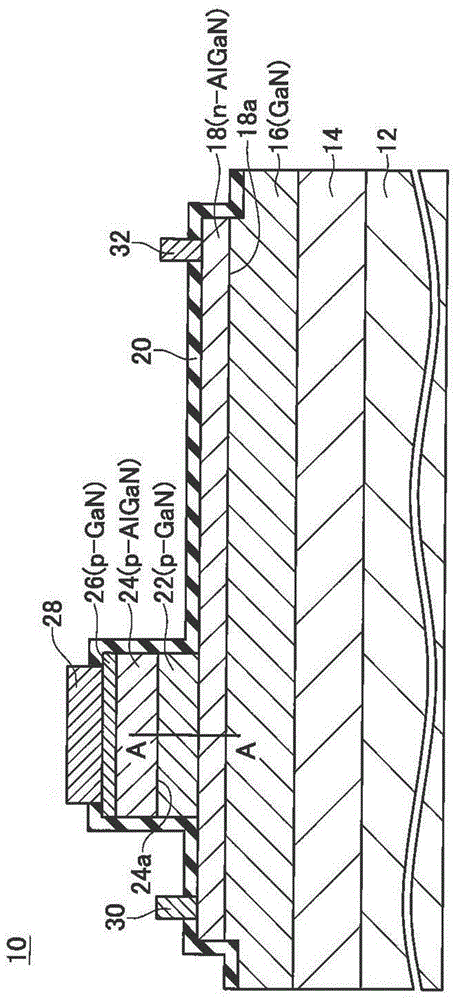
[0021] (Feature 1) The second conductivity type impurity concentration of the third semiconductor layer is higher than the second conductivity type impurity concentration of the fourth semiconductor layer.
[0022] (Feature 2) The first semiconductor layer, the second semiconductor layer, the third semiconductor layer, and the fourth semiconductor layer are nitride semiconductor layers.
[0023] (Feature 3) The first semiconductor layer is a GaN layer, the second semiconductor layer is an n-type AlGaN layer, the third semiconductor layer is a p-type GaN layer, and the fourth semiconductor layer is an Al x Ga 1-x N layers, and 0
[0024] (Feature 4) Alternatively, the first semiconductor layer is a GaN layer, the second semiconductor layer is an n-type or undoped AlGaN l...
PUM
 Abstract
Description
Claims
Application Information