Current-limiting protection circuit

A current-limiting protection and circuit technology, which is applied in the field of circuits, can solve problems such as poor practicability, and achieve the effect of preventing excessive current and enhancing stability and reliability

Active Publication Date: 2015-10-14
EAST CHINA INST OF OPTOELECTRONICS INTEGRATEDDEVICE
4 Cites 7 Cited by

AI-Extracted Technical Summary

Problems solved by technology

However, most of the current limiting protection circuits will derate the output when the current is overloaded, ...

Abstract

The invention is closes a current-limiting protection circuit. The current-limiting protection circuit comprises an overcurrent detection module, a power driving module and a switching control module, wherein when the value of current in a driving signal sub-circuit is higher than an overcurrent value, a fourth triode and an MOS tube form dynamic balance of cascaded negative feedback, so that the MOS tube works in a constant current region and constant current is output, and constant driving power is provided for a load; and an overcurrent signal is output through the overcurrent detection module. According to the current-limiting protection circuit, the current overcurrent value can be rapidly adjusted according to different load requirements, and a condition that the circuit reliability is reduced as the current in the driving signal sub-circuit of a driving power supply is too high, is prevented, so that the technical effects of enhancing the stability and the reliability of a driving circuit is realized, and the current-limiting protection circuit is simple and practical. A triode and MOS tube cascading form is adopted, and the dynamic balance between the triode and the MOS tube is formed through the closed loop negative feedback when the overcurrent occurs, so that the MOS tube works in the constant current region, and the overcurrent signal and the constant current are output; and the constant driving power is provided for the load to keep the capability of the driving circuit, and certain on-line maintaining time can be provided.

Application Domain

Technology Topic

Image

  • Current-limiting protection circuit
  • Current-limiting protection circuit
  • Current-limiting protection circuit

Examples

  • Experimental program(1)

Example Embodiment

[0022] The present invention will be further described below in conjunction with the accompanying drawings. The following examples are only used to illustrate the technical solution of the present invention more clearly, but not to limit the protection scope of the present invention.
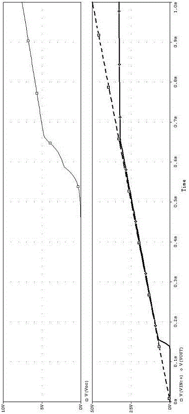
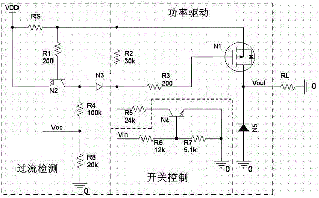
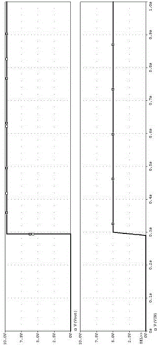
[0023] The invention discloses a current-limiting protection circuit, which is composed of a triode, a MOS tube and several resistors in view of the large output current of the drive circuit, and can quickly adjust the current overcurrent value according to different load requirements. When the current in the drive signal branch is lower than the overcurrent value, the power drive function is realized; when the current in the drive signal branch is higher than the overcurrent value, the triode and the MOS transistor form a dynamic balance of cascaded negative feedback, so that the MOS The tube works in the constant current region, and outputs an overcurrent signal and a constant current to provide a constant drive power for the load, and continue to maintain the circuit enable for a period of time to meet the application requirements of some special occasions.
[0024] Working principle of the present invention: a schematic diagram of a current limiting protection circuit disclosed by the present invention is as follows figure 1 shown. Wherein, the first-stage triode N2 is a PNP transistor, and the MOS transistor N1 is a hexagonal P-channel field effect transistor (HEXFET). RS is a sampling resistor, RL is a resistive load (this design can also be used for inductive loads, and the fast recovery diode N5 acts as a circuit protection when the load is inductive).
[0025] like figure 1 As shown, this current limiting protection circuit is mainly composed of three parts: an overcurrent detection module, a power drive module and a switch control module.
[0026] The overcurrent detection module includes sampling resistor RS, transistor N2, resistors R4, R8. Power supply voltage V DD The sampling resistor RS is respectively connected to the base of the triode N2 and the source of the MOS transistor N1 in the power drive module. The emitter of transistor N2 is connected to the supply voltage V DD. The collector of the transistor N2 is grounded through the resistors R4 and R8, and the collector of the transistor N2 is connected to the gate of the MOS transistor N1 in the power drive module through the diode N3 at the same time. Output voltage drop at overcurrent detection point V oc Divide the voltage through resistors R4 and R8.
[0027] The power drive module includes a MOS transistor N1, a diode N5, a resistor R2, and a resistor R5. The source of MOS transistor N1 is connected to the power supply voltage V DD , the gate of the MOS transistor N1 is connected to the common point of the resistor R2 and the resistor R5 through the resistor R3. The other end of the resistor R2 is connected to the power supply voltage V DD , the other end of the resistor R5 is connected to the switch control module. The drain of the MOS transistor N1 is connected to the output terminal Vout and the cathode of the diode N5 at the same time. The anode of diode N5 is grounded.
[0028] The switch control module includes a transistor N4, resistors R6, R7. Control terminal V in Ground through resistors R6 and R7. The connection point of the resistors R6 and R7 is connected to the base of the transistor N4. The emitter of the transistor N4 and the resistor R7 are both connected to the ground. The collector of the transistor N4 is connected to the power drive module.
[0029] The switch control module controls the circuit to enable, according to the control terminal V in The timing of the input TTL signal realizes the on-off control of the circuit. The base-emitter voltage difference V of the transistor N4 BE4 It can be obtained by dividing the voltage of resistors R6 and R7, as shown in formula (1).
[0030] V BE4 =V in ·R7/(R6+R7) (1)
[0031] When V in When the terminal inputs a low level, there is no voltage difference between the base-emitter of the transistor N4, that is, V BE4 = 0, the transistor N4 is not turned on, and the circuit is not started; when V in When the terminal input high level, V BE4 ≈1.5V, greater than the turn-on voltage V of the transistor N4 BE(set) , the circuit is turned on.
[0032] The power drive module is composed of MOS transistor N1 and so on. Since the sampling resistor RS is very small, the drive power supply voltage V DD The loss on it is negligible, so the source voltage V of the MOS transistor N1 S1 equal to the supply voltage V DD. When the switch control module is enabled, the gate of the MOS transistor N1 can be obtained by dividing the voltage through the resistors R2 and R5, as shown in formula (2).
[0033] V G1 =V DD ·R2/(R2+R5) (2)
[0034] When the gate-source voltage of MOS transistor N1
[0035] V GS1 =V G1 -V S1 (3)
[0036] greater than the turn-on voltage V of N1 GS(th) , the circuit is turned on. Diode N5 is a fast recovery diode, which protects the circuit when the load is inductive. The signal timing diagram when the circuit works normally is as follows: figure 2 shown.
[0037] figure 2 In, take V DD =10V, the circuit works normally. at 0.3 seconds when V in The terminal inputs a high level, the circuit is normally turned on, and provides stable output power for the load.
[0038] according to figure 1 As shown in the circuit principle, the overcurrent detection module detects the circuit current by sampling with a small resistance, and RS is the sampling resistance. According to the circuit connection, the voltage V across the sampling resistor RS RS Equal to the base-emitter voltage V of the transistor N2 BE2 and the voltage across resistor R1 V R1 The sum of the resistance R1 is the triode base protection circuit, and the current flowing through it is very small, so there are:
[0039] V BE2 ≈V RS (3)
[0040] When the driving circuit is working normally, the current I flowing through the sampling resistor RS RS Small, according to Ohm's law, we can know the voltage V across the sampling resistor RS RS Smaller, at this time the base-emitter voltage drop V of the transistor N2 BE2 less than its turn-on voltage V BE(set) , the circuit does not enter the over-current protection. When the drive voltage of the circuit is too high and an overcurrent phenomenon occurs, the voltage I across the sampling resistor RSRS increases accordingly, when V BE2 ≥V BE(set) , the transistor N2 is turned on. At this time, the power supply voltage directly reaches the gate of the MOS transistor N1 after passing through the transistor N2 and the diode N3, and the voltage difference between the gate and the source of the MOS transistor V GS1 =0V, MOS transistor N1 is turned off. After the MOS transistor N1 is turned off, the circuit where the sampling resistor RS is located is disconnected, and I RS = 0A, the transistor N2 is closed. The whole circuit achieves dynamic balance in the closed-loop negative feedback, the base-emitter V of the transistor N1 BE2 At the zero point of turn-on and turn-off, V BE2 =V BE(set). MOS transistor gate-source voltage V GS1 =V GS(thmax) , MOS transistor N1 works in the constant current region, and the circuit outputs constant current when the circuit is over-current, continuously providing constant power to the load.
[0041] At this point, the output current expression when the circuit is overcurrent is shown in formula (4).
[0042] I e = V e R L = V B E ( s e t ) R S - - - ( 4 )
[0043] Then, when the circuit is over-current, the output voltage is shown in formula (5)
[0044] V e = V B E ( s e t ) R S · R L - - - ( 5 )
[0045] When the circuit is not over-current, the collector voltage V of transistor N2 C2 and MOS transistor N1 gate voltage V G1 equal, ie
[0046] V C2 =V E2 -|V GS1 |=V DD -|V GS(thmax) | (6)
[0047] Then, the output voltage drop V at the overcurrent detection point oc It can be obtained by dividing the voltage through resistors R4 and R8, as shown in formula (7).
[0048] V oc =V C2 ·R8/(R4+R8) (7)
[0049] Then, the output waveforms of the current limiting protection circuit under different driving power supply voltages are as follows: image 3 shown.
[0050] The driving power supply voltage is set to increase linearly from 0 to 50V, such as image 3 Shown by the dotted line. Depend on image 3 It can be seen that when the driving power supply is undervoltage, the circuit is not turned on; when the driving power supply voltage is too large and the output is overcurrent, the current limiting protection function is turned on, and the circuit outputs a constant current. At this time, there is a signal output at the overcurrent detection point. In order to better observe the over-current detection signal, a buffer can be connected to the over-current detection terminal, and an appropriate threshold can be selected to shape the over-current detection signal and output in the form of high and low levels, which will not be further discussed in this patent.
[0051] The above is only a preferred embodiment of the present invention, it should be pointed out that for those of ordinary skill in the art, without departing from the technical principle of the present invention, some improvements and modifications can also be made. It should also be regarded as the protection scope of the present invention.

PUM

no PUM

Description & Claims & Application Information

We can also present the details of the Description, Claims and Application information to help users get a comprehensive understanding of the technical details of the patent, such as background art, summary of invention, brief description of drawings, description of embodiments, and other original content. On the other hand, users can also determine the specific scope of protection of the technology through the list of claims; as well as understand the changes in the life cycle of the technology with the presentation of the patent timeline. Login to view more.

Similar technology patents

Speed regulator for blender

Owner:珠海市振业混凝土有限公司

Driving power supply of wind turbine generator pitch variable system

InactiveCN107888076AAvoid excessive currentImprove current suppressionDc-dc conversionWind energy generationCurrent limitingInterference resistance
Owner:CHONGQING KK QIANWEI WINDPOWER EQUIP

Classification and recommendation of technical efficacy words

  • Avoid excessive current
  • Improve stability and reliability

Fuel cell electric vehicle power device with super-capacitor

InactiveCN105730256AAvoid excessive currentPropulsion by capacitorsPropulsion by batteries/cellsElectric machineryCapacitance
Owner:陆玉正

Multi-pin grounding shielded wire

InactiveCN106297977AReduce circulationAvoid excessive currentInsulated cablesCarbon-silicon compound conductorsPower flowActual use
Owner:JIANGSU HENGTONG ELECTRONICS CABLE TECH CO LTD

Receiver system

ActiveUS20140119479A1Improve stability and reliabilityGain controlAmplitude demodulation by non-linear two-pole elementsVIT signalsReceiver system
Owner:EM MICROELECTRONIC-MARIN
Why Eureka
Try Eureka